
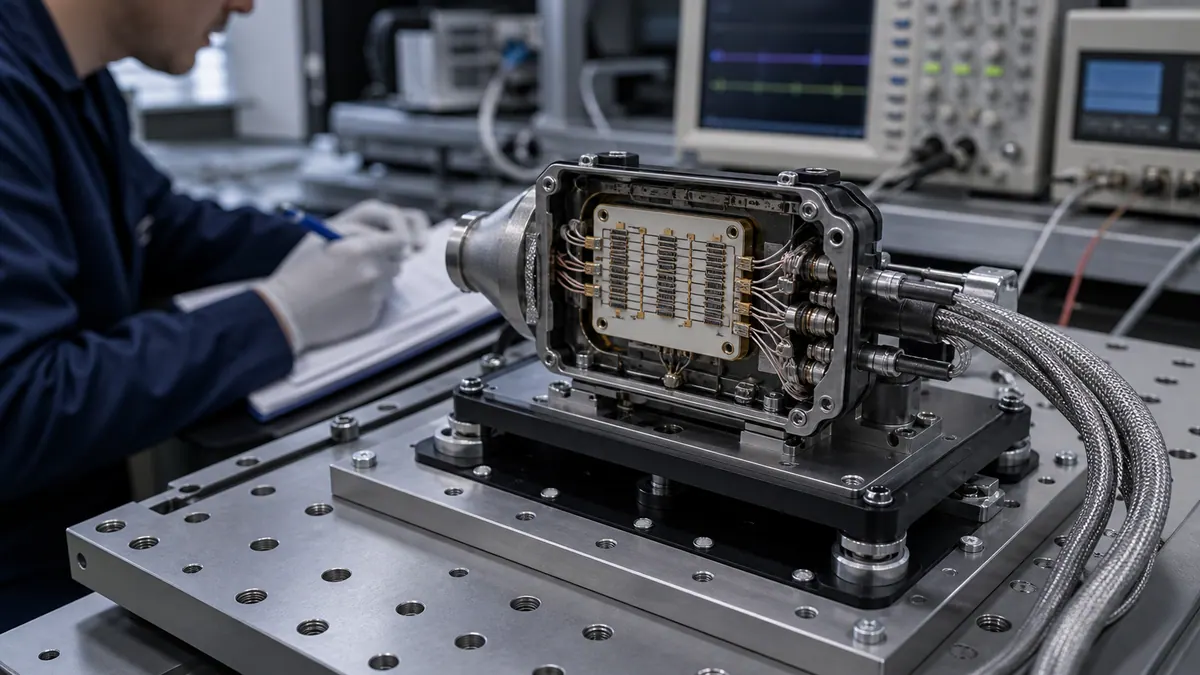
Alumina and aluminum nitride are common substrates for thick film hybrid circuits because they combine electrical insulation, dimensional stability, thermal performance, and compatibility with fired conductor, resistor, and dielectric paste systems. For higher integration, the design can go beyond a single printed conductor layer.
Hybrid circuit structures
- Single-side or double-side conductor printing.
- Multilayer conductor and dielectric structures for compact routing.
- Metallized holes or through connections when the substrate and process route support them.
- Printed resistor networks with either designed-as-fired values or optional laser/functional trimming.
- Gold, silver, palladium-silver, platinum-gold, or other conductor systems selected by assembly method.
Fine-line thick film
Fine-line thick film aims to narrow conductor geometry while staying compatible with thick film process logic. It can be useful for compact hybrid circuits, high-frequency layouts, interdigitated electrodes, small sensor patterns, and dense ceramic modules. Feasibility depends on screen technology, paste rheology, substrate quality, registration, firing profile, and inspection method.
Design review points
- Minimum track and gap required by the selected paste and screen process.
- Substrate thickness, flatness, surface finish, and outline tolerance.
- Pad-to-edge, hole-to-edge, and pad-to-track clearances.
- Whether resistors are non-trimmed, passive trimmed, or functionally trimmed.
- Assembly method: soldering, wire bonding, die attach, connector, or spring contact.
- Application field: automotive, medical, railway, aerospace, RF, industrial, or research module.
Non-trimmed and trimmed designs
Not every thick film resistor should show a trim cut. Some products are designed as non-trimmed resistor or heater patterns where the value range is accepted after controlled printing and firing. Other precision circuits require passive or functional trimming. The drawing and product photo should match the actual manufacturing route.