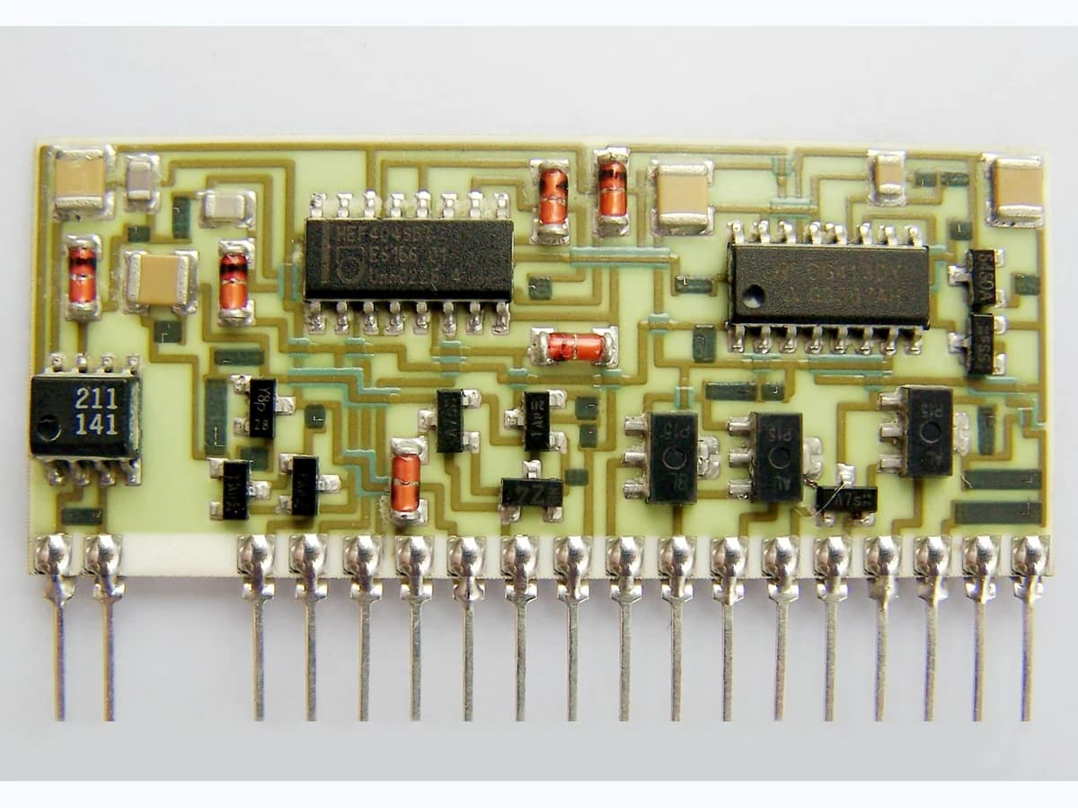
Printed circuit and substrate definition
Review ceramic material, outline, datums, printed conductors, resistors, dielectric or protection, openings, tolerances, print sequence, firing compatibility, and inspection access.

Hybrid Circuit Engineering
Custom thick film hybrid circuits can integrate printed conductors, resistors, dielectric or protective layers, mounted components, die interfaces, wire bonds, and external terminals on a compact ceramic platform. Send the drawing, artwork, BOM or die map, electrical and thermal conditions, assembly notes, quantity, and validation plan so engineering can review the complete build.
Verified capability review
Thick Film Hybrid Circuit is shown against approved company capability control sheets.
Capability source: approved company category control sheets. Final values remain drawing- and sample-controlled.
| Parameter | Standard capability | Engineering review range | Final release |
|---|---|---|---|
| Substrate Material | 96% Alumina (Al₂O₃) standard route | 99% / 99.6% alumina or AlN through material and process review | Approved material specification, drawing, and incoming criteria |
| Board Thickness | 0.25–3.0 mm | Thickness inside 0.25–3.0 mm is checked against outline, flatness, holes, handling, and firing | Approved material specification, drawing, and incoming criteria |
| Conductor System | Silver (Ag) / Silver-Palladium (Ag-Pd) | Pt-Ag, Au, bonding, soldering, contact, and high-temperature routes by compatible stack review | Approved material stack, assembly interface, and sample |
| Resistor System | RuO₂ thick film | Paste family, sheet resistance, geometry, refire sequence, and trim allowance by circuit target | Released drawing and approved sample |
| Conductor Thickness | 10–25 µm | Value inside 10–25 µm is selected for print build, firing, current path, and assembly | Released drawing, DFM approval, and first-article inspection |
| Resistor Tolerance | ±1% standard | ±0.5% available after geometry, material, trimming, and measurement review | Released drawing and approved sample |
| Parameter | Standard capability | Engineering review range | Final release |
|---|---|---|---|
| Firing Temperature | Up to 850°C | The peak profile is paste- and stack-specific within the approved route; later refires are reviewed together | Approved material-process route and production traveler |
| Thermal Conductivity | ≥24 W/m·K, 96% alumina reference | Alternative alumina grade or AlN route by approved material certificate and system thermal review | Released drawing and approved sample |
| Minimum Line/Space | ≥100 µm | Geometry at the ≥100 µm controlled capability is checked for paste, screen, registration, overlap, edge clearance, and yield | Released drawing, DFM approval, and first-article inspection |
| Board Size | Up to 120 × 120 mm | Larger than 120 × 120 mm by panel, flatness, handling, firing, and inspection review | Released drawing, DFM approval, and first-article inspection |
| Surface Finish | HASL / ENIG / ENEPIG | Finish selected for soldering, bonding, contact, storage, and downstream thermal exposure | Approved material stack, assembly interface, and sample |
| Dielectric Strength | ≥15 kV/mm | Product withstand voltage is derived from dielectric material, fired thickness, clearances, interfaces, and test method | Released insulation stack and agreed IR/withstand test plan |
Four review controls connect the printed ceramic circuit, component or die assembly, terminals, electrical duty, and validation plan. Supplied photographs support visible-feature review; final materials, dimensions, performance, process limits, and records remain project-controlled.
Review ceramic material, outline, datums, printed conductors, resistors, dielectric or protection, openings, tolerances, print sequence, firing compatibility, and inspection access.
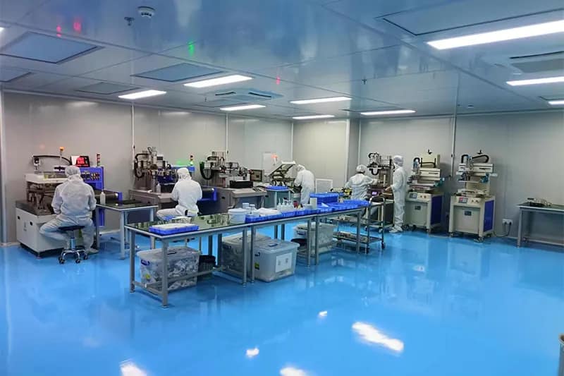
Control artwork revision, layer-to-layer alignment, paste and screen selection, drying, firing, pad openings, component keep-outs, fiducials, and measurable release limits.
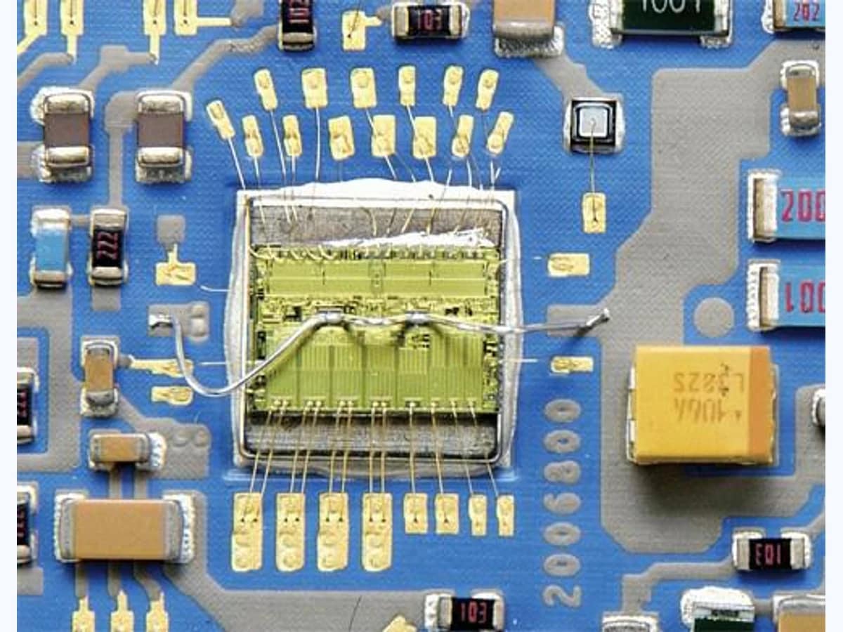
Connect the BOM, packages, die map, attach system, wire bonds, pad finish, terminal form, housing, cleaning, protection, and rework rules to one assembly route.
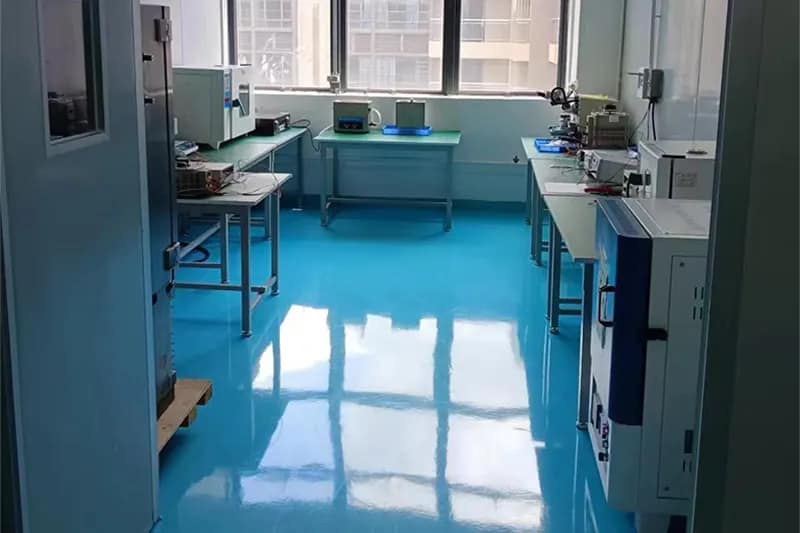
Select visual, dimensional, electrical, functional, bond, cleanliness, thermal, environmental, traceability, and packing checks with agreed limits, sampling, and records.
These application illustrations show conditional engineering directions. Suitability depends on the released circuit, assembly, electrical, thermal, mechanical, environmental, and validation requirements.
Application images are engineering illustrations, not customer projects, production records, or evidence of a released design. Suitability is confirmed only after the drawing, interfaces, operating conditions, risks, and validation plan are reviewed.
 Application illustration
Hybrid circuits can be reviewed for compact sensor interfaces after signal levels, resistor functions, input protection, calibration, connector geometry, environment, and functional-test limits are released.
Review sensor inputs Application illustration
A ceramic hybrid assembly may support compact control electronics when the schematic, I/O, isolation, terminals, component loading, thermal boundary, enclosure, and validation route are defined.
Review control inputs Application illustration
Printed routing, mounted components, die attach, wire bonds, and terminal interfaces can be reviewed for compact carriers after the complete stack, assembly process, heat path, cleanliness, and reliability plan are released.
Review hybrid inputsThe supplied photographs visibly confirm multiple hybrid-circuit formats, printed routing and pads, mounted components, a long row of metal leads, and a macro view with a die area and fine wire bonds. They do not establish substrate grade, paste chemistry, dimensions, BOM identity, bond material or strength, electrical function, operating conditions, lot history, inspection results, or shipment status.
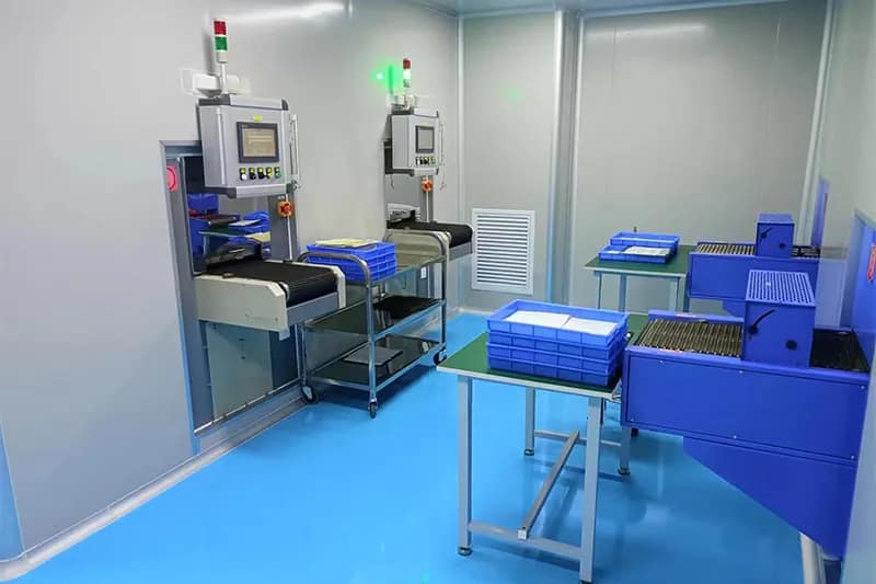
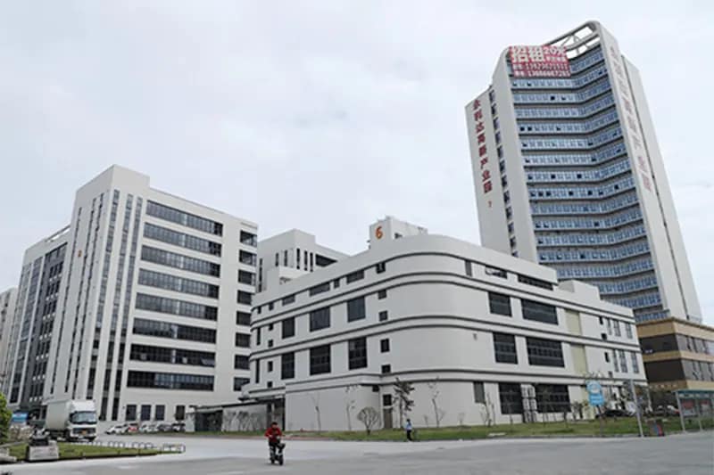
Company resources support thick film screen printing, controlled firing, laboratory inspection, and managed production in Dongguan.
The applicable ceramic, printed system, assembly route, tests, sampling, traceability, and acceptance records are confirmed for each released project.
Short answers for quotation planning; released drawings and validation requirements remain controlling.
Engineering reviews the ceramic substrate, printed conductor, resistor and dielectric requirements, component and die interfaces, attachment and wire-bond process, terminals, electrical and thermal duty, enclosure, environment, inspection, traceability, quantity, and validation plan as one released assembly. The exact route follows the customer drawing, BOM, artwork, and acceptance criteria.
The available product views show examples with mounted components and a visible die-and-wire-bond area, so those interfaces can be reviewed. Feasibility still depends on the BOM, package data, pad finish, die map, attach system, bond-wire and pad compatibility, thermal profile, cleaning, protection, workmanship standard, inspection, and qualification requirements.
Send the dimensioned drawing, layer artwork, ceramic requirement, net or schematic information, BOM and package data, die map when applicable, conductor and resistor targets, component attachment and wire-bond notes, terminal definition, electrical and thermal conditions, enclosure and environment, prototype and production quantities, inspection plan, and required records.
No. They confirm visible product form, printed routing, mounted parts, a lead row, and a die-and-wire-bond area. They do not prove material identity, dimensions, values, bond strength, electrical function, operating temperature, cycling life, lot traceability, or shipment status. Those claims require authorized drawings, records, and project-specific results.
Send enough information to connect the ceramic circuit, printed layers, BOM or die map, assembly interfaces, terminals, electrical and thermal duty, environment, validation plan, and order scope. Sample photographs can begin a review, but the production build must be drawing-controlled.
PDF, DWG, DXF, STEP, Gerber, ZIP, Excel, Word, or sample photos are accepted.
The drawing-upload form loads as you reach this section.