Ceramic thick film circuits
Alumina and selected AlN projects with printed conductors, resistors, dielectric features, protective layers, and assembly interfaces.

About Chipsimple
ThickFilmPCB is the engineering and RFQ site of Dongguan Jianchuang Electronic Technology Co., Ltd., presented under the Chipsimple name. From our Dongguan operation, the team reviews custom ceramic circuits, printed resistors, sensor cards, and thick film heaters against the drawing, material system, assembly, operating environment, and evidence required for prototype and repeat-production release.
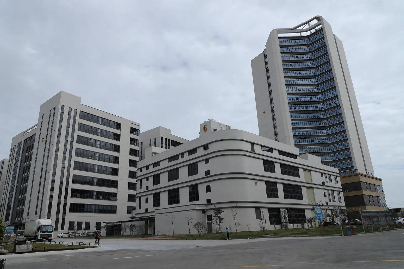
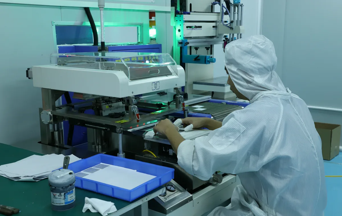
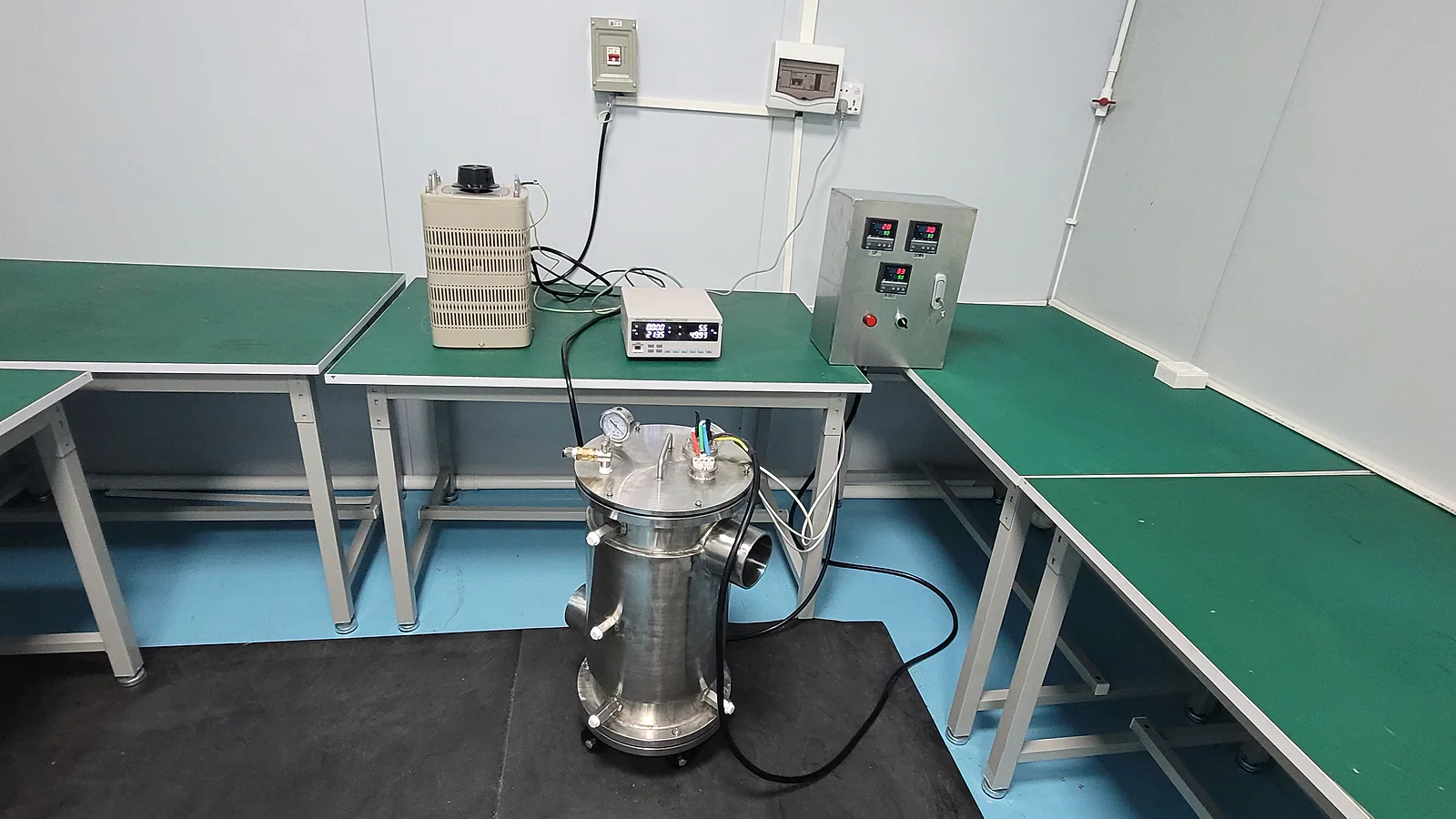
Chipsimple connects overseas OEM engineers, sourcing teams, and product developers with the Dongguan manufacturing and engineering-review team. The job is straightforward: understand what the part must do, identify the right material and process route, expose open risks early, and define the evidence needed for sample and production release.
The route is not selected from a product name alone. Substrate, printed material system, geometry, assembly, environment, measurement method, quantity, and required evidence are reviewed together before a project-specific specification is released. We do not present a single line width, tolerance, power, voltage, temperature, or lifetime as universal across every material stack.
These four company-supplied images come from the 2026 company presentation and the approved site reference-image library. They document workplace and equipment context; they do not by themselves prove a specific customer lot, universal process limit, calibration status, measurement result, or cleanroom classification.
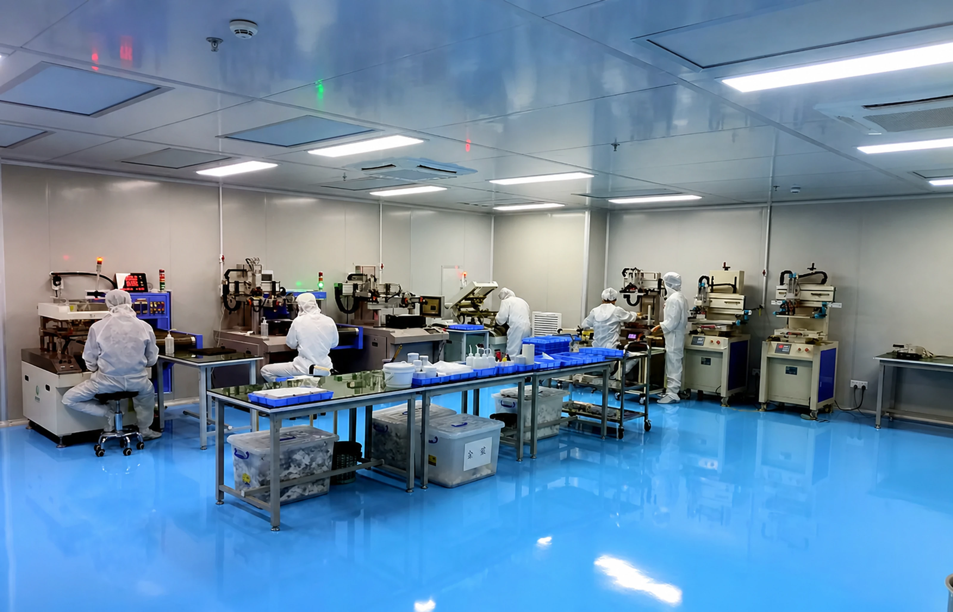
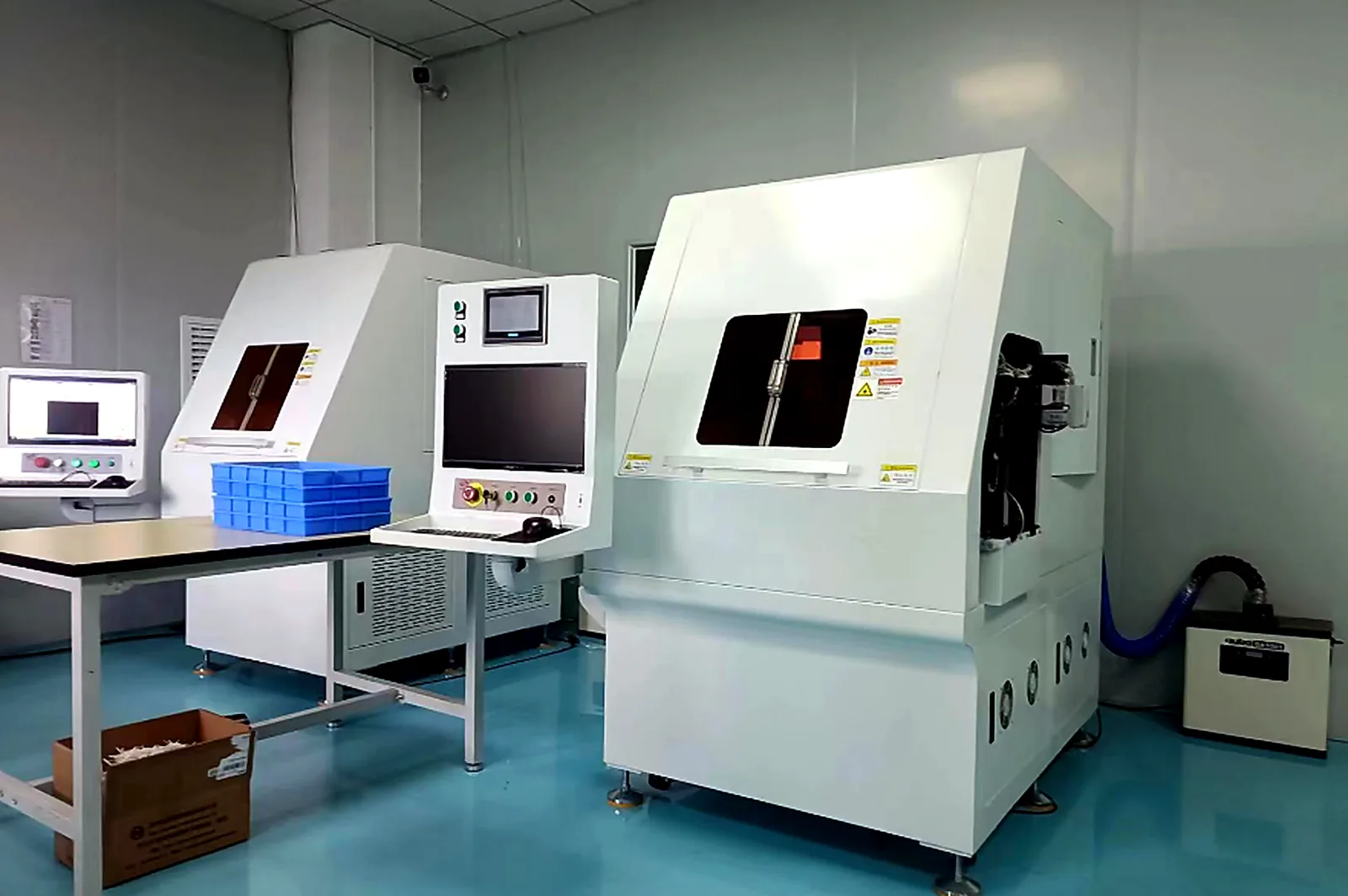
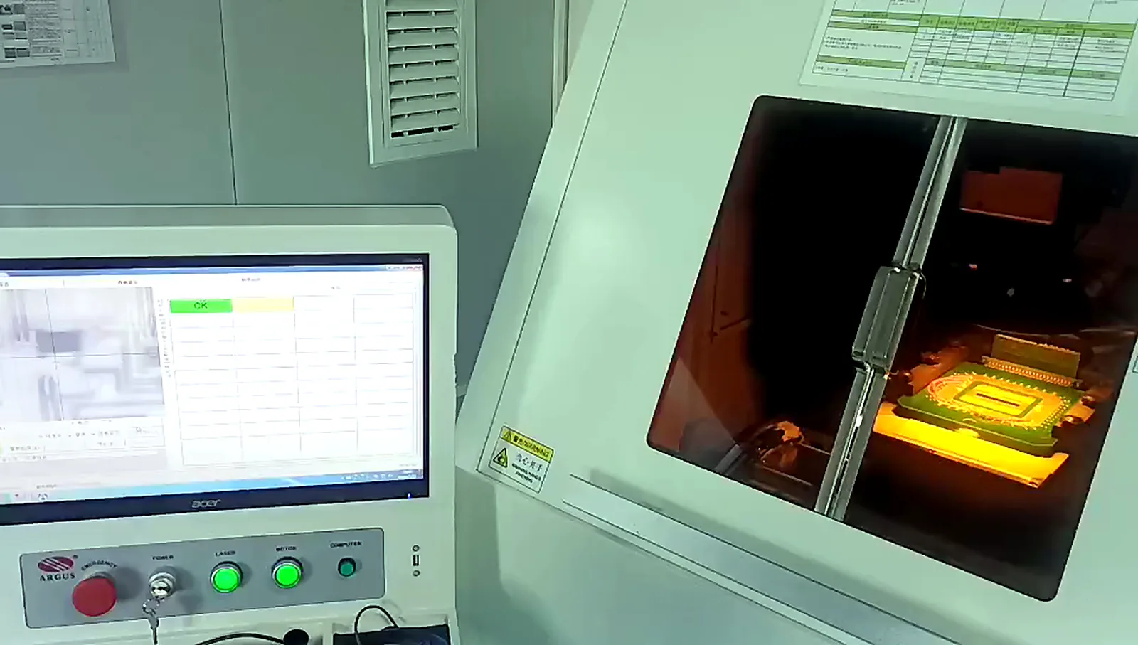
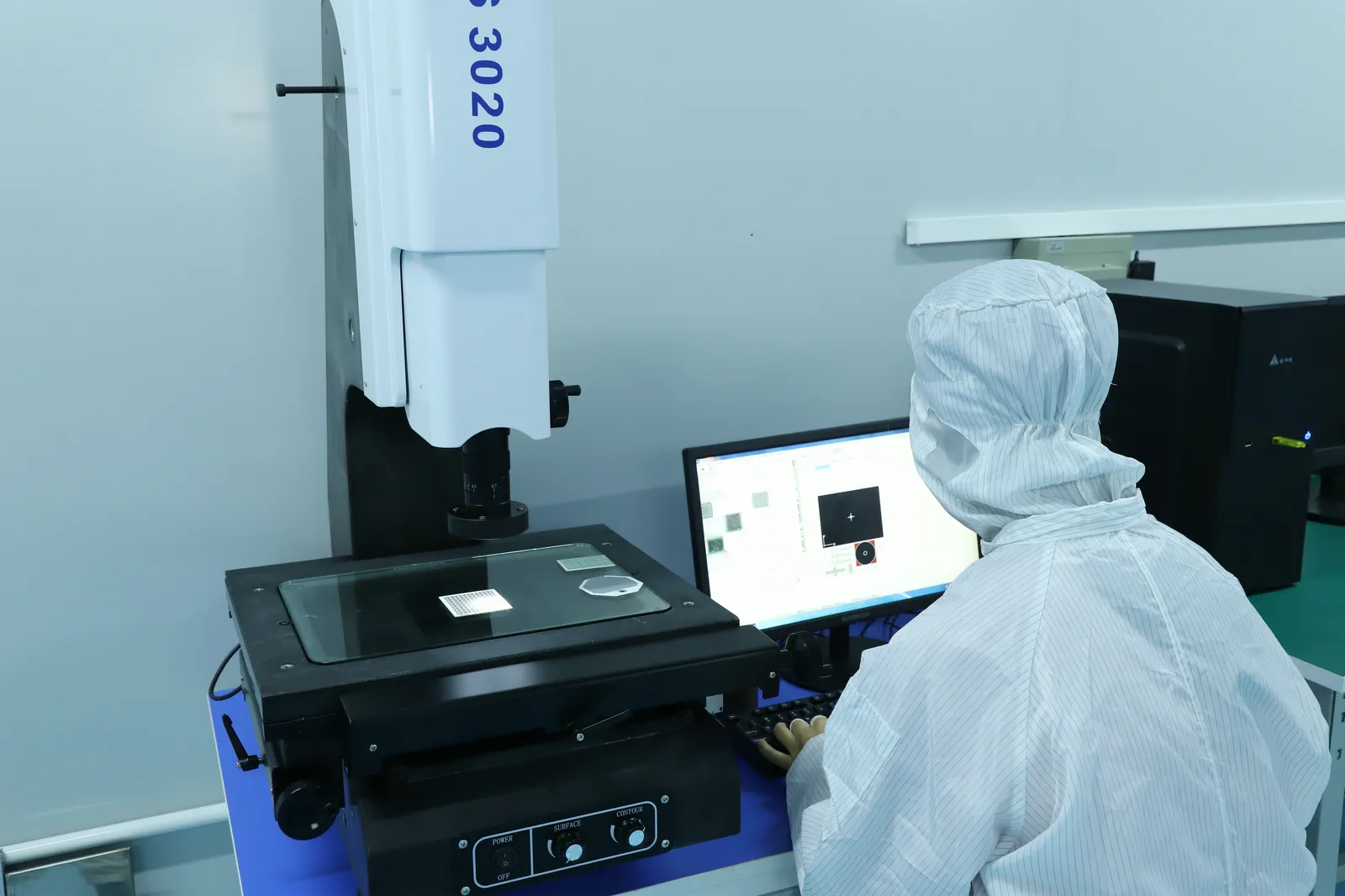
For a critical program, request the applicable equipment route, measurement method, calibration evidence, inspection record, and lot-document requirements during RFQ review.
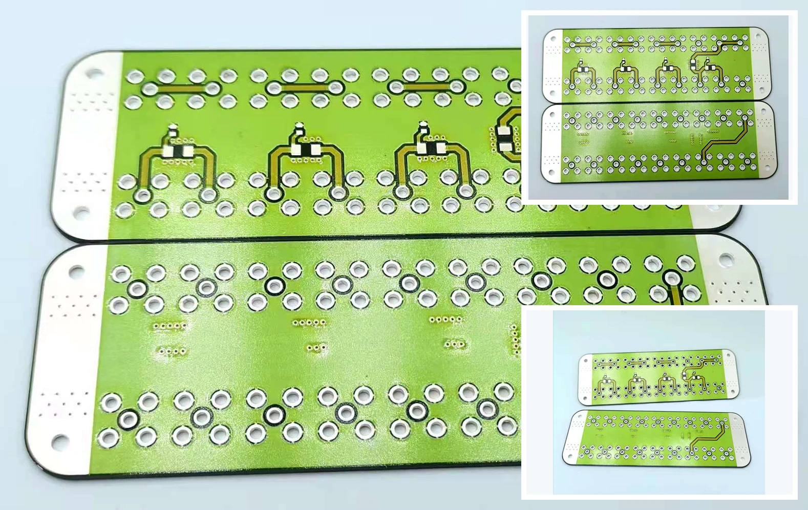
Alumina and selected AlN projects with printed conductors, resistors, dielectric features, protective layers, and assembly interfaces.
Fixed values, matched ratios, sensor tracks, dividers, and custom geometries reviewed with trimming, loading, and measurement conditions.
Fuel, oil, throttle, level, and position projects reviewed with track geometry, contact interface, output curve, media exposure, and wear requirements.
Ceramic, stainless-steel, and other reviewed heater routes defined by voltage, resistance, power, heat path, sensing, insulation, mounting, and duty cycle.
Confirm the drawing, function, material, assembly, environment, volume, and required evidence.
Resolve artwork, compatible materials, processing, trimming, terminals, protection, and inspection.
Build representative parts under the released artwork and process sequence.
Check dimensions, appearance, electrical, thermal, or sensor function by the agreed method.
Lock revisions, materials, sampling, traceability, packaging, and change communication.
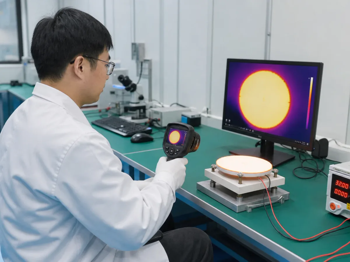
A ceramic circuit, printed sensor track, resistor network, and heater do not share one universal release plan. The drawing and application determine which checks are needed and what record is useful.
Open the originals to review the holder, printed dates, scope, sample description, methods, and conclusions. A report for one sample is not presented as blanket certification for every product.
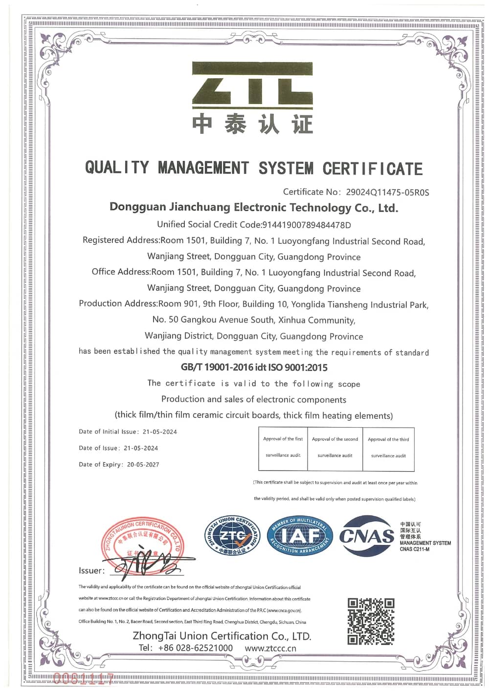
Certificate 29024Q11475-05R0S names Dongguan Jianchuang Electronic Technology Co., Ltd. and has a printed expiry of 20 May 2027; surveillance conditions apply. The original preserves the issuer's registered, office, and production address wording.
Open certificate PDF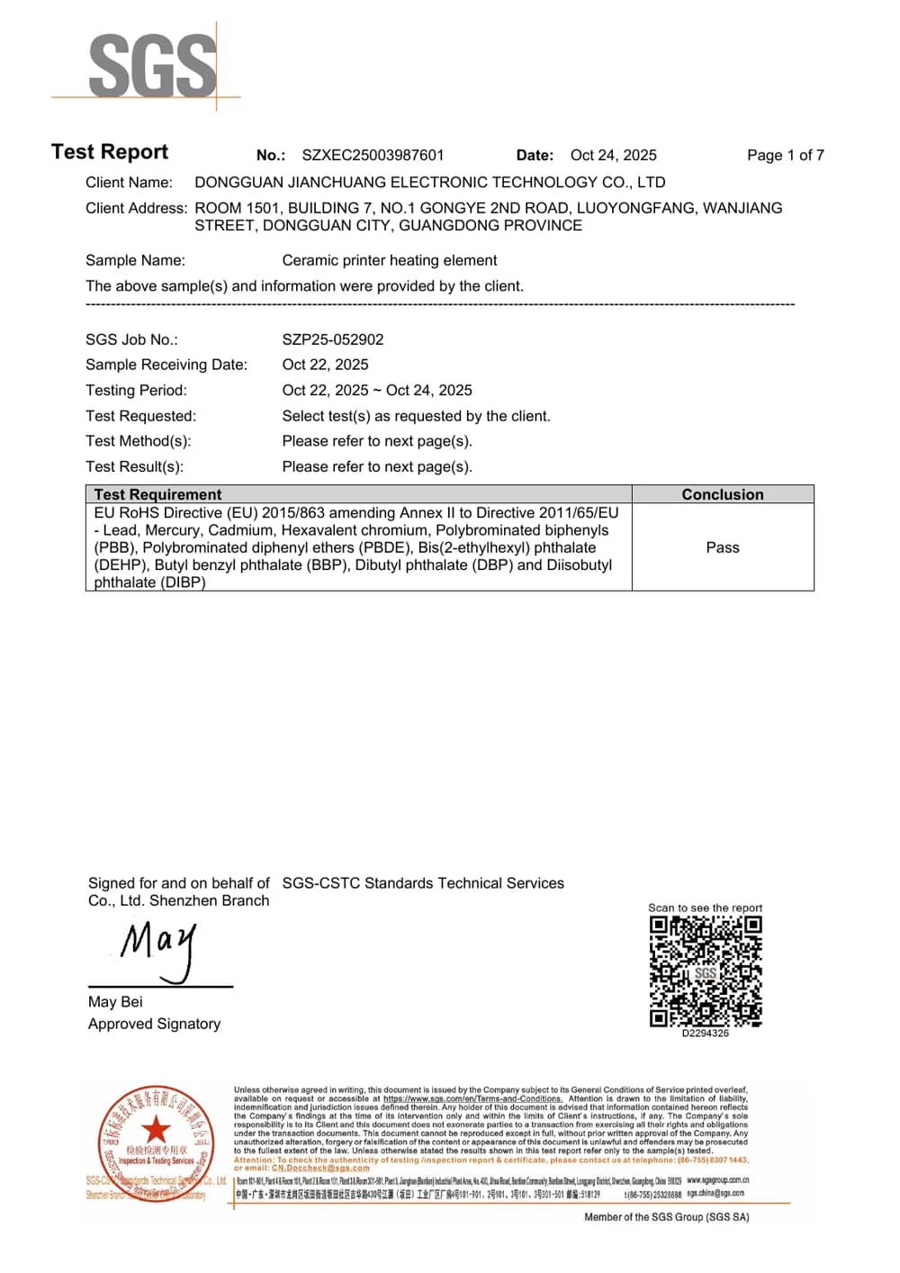
Report SZXEC25003987601, dated 24 October 2025, covers the identified ceramic printer heating-element sample; conclusion: Pass.
Open 7-page PDF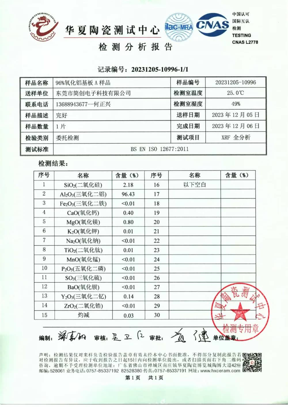
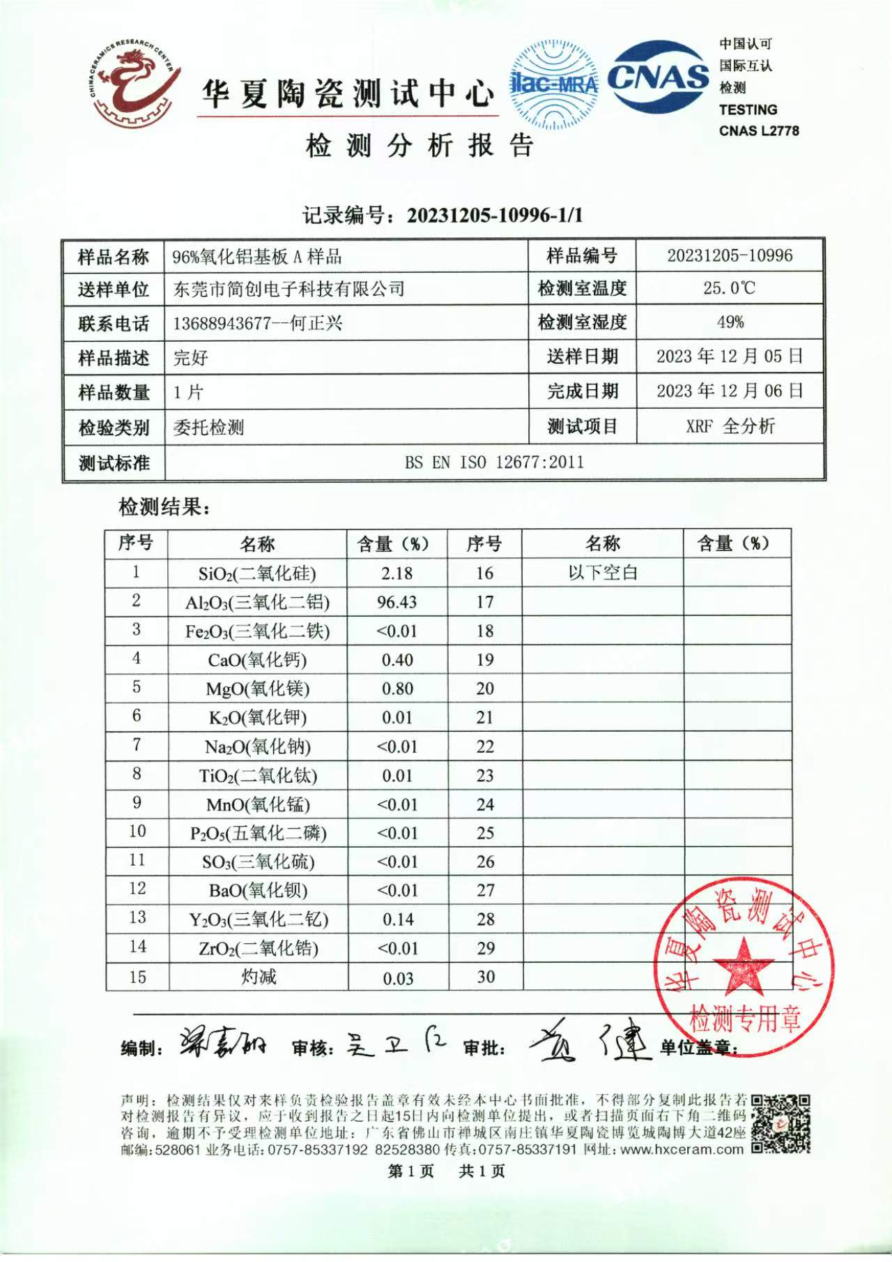
XRF record 20231205-10996-1/1 reports Al₂O₃ at 96.43% for the single identified 96% alumina substrate sample.
Download reportTechnical content governance
Engineering and technical content review
Scope: Ceramic thick film circuits, printed resistors, sensor circuits, and thick film heaters. Review uses company-source process evidence, published technical references, and drawing-controlled manufacturing requirements.
Technical articles show their factual online publication and latest review dates. A named individual reviewer is shown only when a verifiable name, role, and review record are available. Product limits remain subject to the released drawing, material system, assembly, operating conditions, and agreed test method.
Include substrate, dimensions, printed functions, resistance or thermal target, assembly, environment, quantity, schedule, and required tests. Unknown inputs can be identified during review.