Array material and value ranges
Select ceramic, resistor paste families, conductor system, print and firing sequence, multiple value ranges, protection, and compatible refire limits for the array.

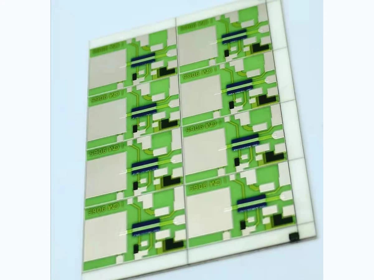
Precision-adjusted printed resistor array
Laser-trimmed thick film resistor arrays integrate multiple printed elements and adjust selected values or ratios under controlled measurement. Chipsimple reviews array topology, paste families, target values, tolerance, ratios, TCR tracking, trim allowance and sequence, probe access, loading, protection, thermal coupling, stabilization, and inspection before release.
Verified capability review
Laser-Trimmed Thick Film Resistor Array is shown against approved company capability control sheets.
Capability source: approved company category control sheets. Final values remain drawing- and sample-controlled.
| Parameter | Standard capability | Engineering review range | Final release |
|---|---|---|---|
| Substrate / Thickness | 96% / 99% Alumina / AlN; 0.25–3.0 mm | 96%/99% alumina or AlN within 0.25–3.0 mm, selected for thermal path, voltage, flatness, assembly, and firing | Approved material specification, drawing, and incoming criteria |
| Resistor System | RuO₂ / Cermet | RuO₂ or cermet selected for value, sheet resistance, TCR, load, stability, conductor, and firing compatibility | Released drawing and approved sample |
| Sheet Resistance | 1 Ω/□–1 MΩ/□ paste-family reference | Select within the 1 Ω/□–1 MΩ/□ paste-family reference after value, geometry, aspect ratio, and trim review | Released electrical limits, measurement method, and approved sample |
| Conductor System | Ag / Ag-Pd / Au | Ag, Ag-Pd, or Au selected for termination, bonding, soldering, voltage, environment, and firing | Approved material stack, assembly interface, and sample |
| Resistor Film Thickness | 8–15 µm fired typical | Within 8–15 µm fired typical, print build, firing, geometry, value distribution, and trimming are controlled | Released drawing, DFM approval, and first-article inspection |
| Firing Temperature | Up to 850°C | Peak up to 850°C; the actual profile, atmosphere, dwell, and refire sequence follow the selected paste system | Approved material-process route and production traveler |
| Parameter | Standard capability | Engineering review range | Final release |
|---|---|---|---|
| Resistance Value | 10 Ω–10 MΩ typical | Within 10 Ω–10 MΩ typical, nominal, ratio, reference temperature, voltage, and measurement method are defined | Released electrical limits, measurement method, and approved sample |
| Resistance Tolerance | ±1% standard | ±0.5% available after paste, geometry, trim allowance, TCR, stability, and measurement review | Released electrical limits, measurement method, and approved sample |
| TCR | ±100–200 ppm/°C typical | Within ±100–200 ppm/°C typical, define temperature interval, tracking, stabilization, and measurement method | Released electrical limits, measurement method, and approved sample |
| Laser Trimming | Passive / Active | Passive or active trimming with approved kerf, cut geometry, stopping rule, test condition, and post-trim protection | Released drawing and approved sample |
| Power / Working Voltage | By geometry and thermal design | Released from geometry, substrate, heat path, ambient, duty, pulse, clearance, field grading, and protection | Approved electrical-thermal design and instrumented prototype validation |
| Protection | Glass overglaze / Passivation | Glass overglaze or passivation selected for trim access, assembly, moisture, contamination, voltage, and temperature | Approved material stack, assembly interface, and sample |
A stable trimmed array needs a complete electrical and process error budget. Engineering connects fired-value distribution, resistor geometry, trim kerf and direction, current density, conductor resistance, element interaction, probe force, measurement voltage, stabilization, passive or active sequence, thermal coupling, protection, post-trim checks, and long-term drift requirements.
Select ceramic, resistor paste families, conductor system, print and firing sequence, multiple value ranges, protection, and compatible refire limits for the array.
Release each resistor, terminal, common node, trim allowance, safe cut area, conductor clearance, probe pad, identification, and dimensional datum in controlled artwork.
Define target values or ratios, tolerance, TCR, measurement voltage, circuit bias if active, probe sequence, stabilization, loading, temperature, and channel calculations.
Specify cut acceptance, remeasurement, ratio checks, isolation, visual inspection, protection, thermal or environmental stabilization, sampling, data retention, and failure limits.
Trimmed arrays fit precision sensing and control when the topology, probe access, thermal coupling, measurement sequence, and drift requirements are controlled from design through release.
Application images are engineering illustrations, not customer projects, production records, or evidence of a released design. Suitability is confirmed only after the drawing, interfaces, operating conditions, risks, and validation plan are reviewed.
 Application illustration
Precision signal paths require defined values, ratios, loading, temperature, calibration, cleanliness, drift, and traceable measurement under production-intent conditions.
Review application inputs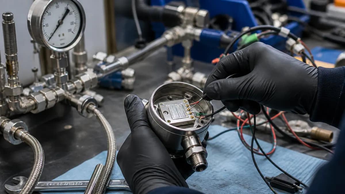 Application illustration
Sensor arrays need application-specific ratio, TCR tracking, vibration, temperature, electrical transients, calibration, traceability, and validation.
Review application inputs Application illustration
Medical instrumentation requires controlled error budgets, loading, calibration, material documentation, environment, traceability, and risk-based validation.
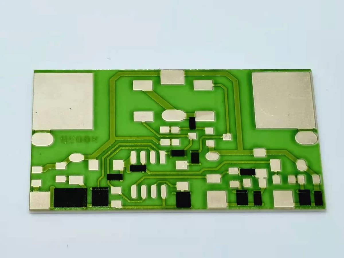
Review application inputsThe verified photographs show real green ceramic arrays and panels with printed resistor and conductor regions, large terminal areas, repeated layouts, and panelization features. No trim cut is clearly established by these surface views, so laser-trim status, cut geometry, values, ratios, tolerance, and measurement records remain controlled process and test facts.
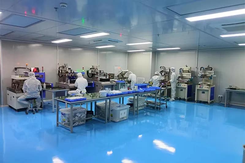
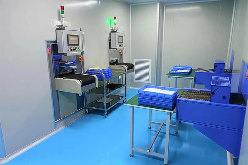
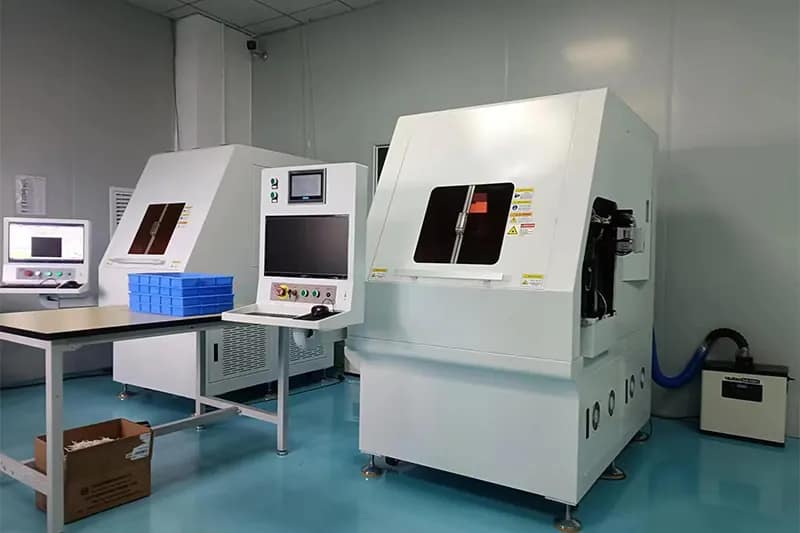
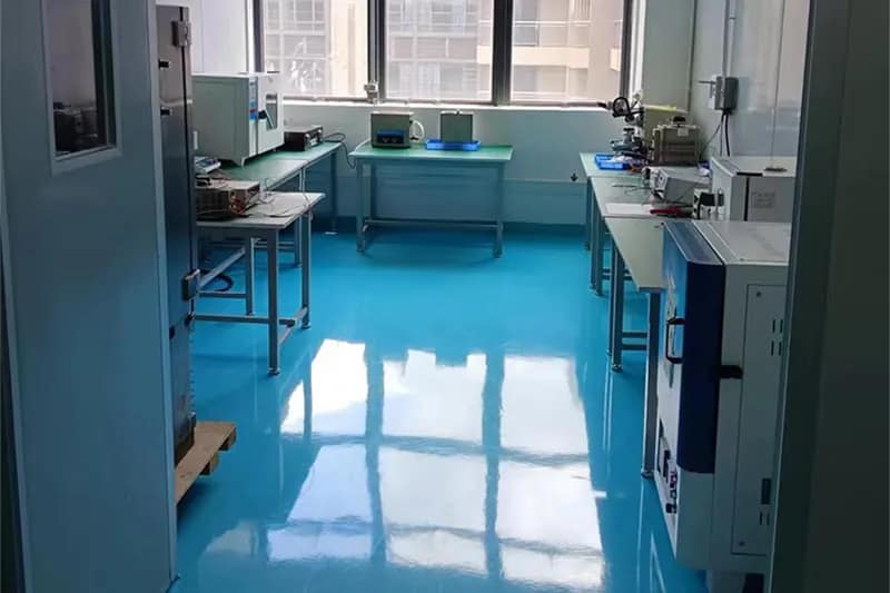
Chipsimple supports resistor printing, controlled firing, laser trimming, and laboratory inspection in Dongguan.
Trimmed-array projects release the topology, value table, trim geometry and sequence, probe method, stabilization, post-trim tests, protection, sampling, traceability, and acceptance records together; precision claims depend on the approved measurement conditions.
Short answers for quotation planning; released drawings and validation requirements remain controlling.
Provide array schematic and artwork, every target value and ratio, tolerance, TCR and tracking, fired-value window, trim allowance and forbidden areas, passive or active circuit condition, probe points, measurement voltage, stabilization, channel sequence, loading, protection, environment, and data-retention needs.
No. They are practical category-level selection values, not a released product specification. Material compatibility, geometry, print build, electrical loading, assembly, environment, inspection method, and expected volume can narrow the usable window. Final values are confirmed against the controlled drawing and approved project conditions.
Control pre-trim measurement, probe contact, stabilization, trim sequence and limits, post-trim value and ratio checks, visual cut criteria, isolation, protection, remeasurement, TCR or environmental conditioning, drift, sampling, and traceable data. Active trimming must use the released circuit bias and calculation method.
Send the controlled drawing or artwork, dimensions and tolerances, material preference, electrical targets, assembly interface, operating environment, validation requirements, prototype quantity, annual volume, and schedule. Include the array schematic, value and ratio table, fired window, trim limits, probe points, passive or active conditions, stabilization, and data needs.
Send the complete array topology and measurement definition with the artwork. Fired-value margin, trim geometry, probe access, passive or active conditions, sequence, stabilization, ratios, protection, loading, and data retention determine the achievable production route and inspection plan.
PDF, DWG, DXF, STEP, Gerber, ZIP, Excel, Word, or sample photos are accepted.
The drawing-upload form loads as you reach this section.