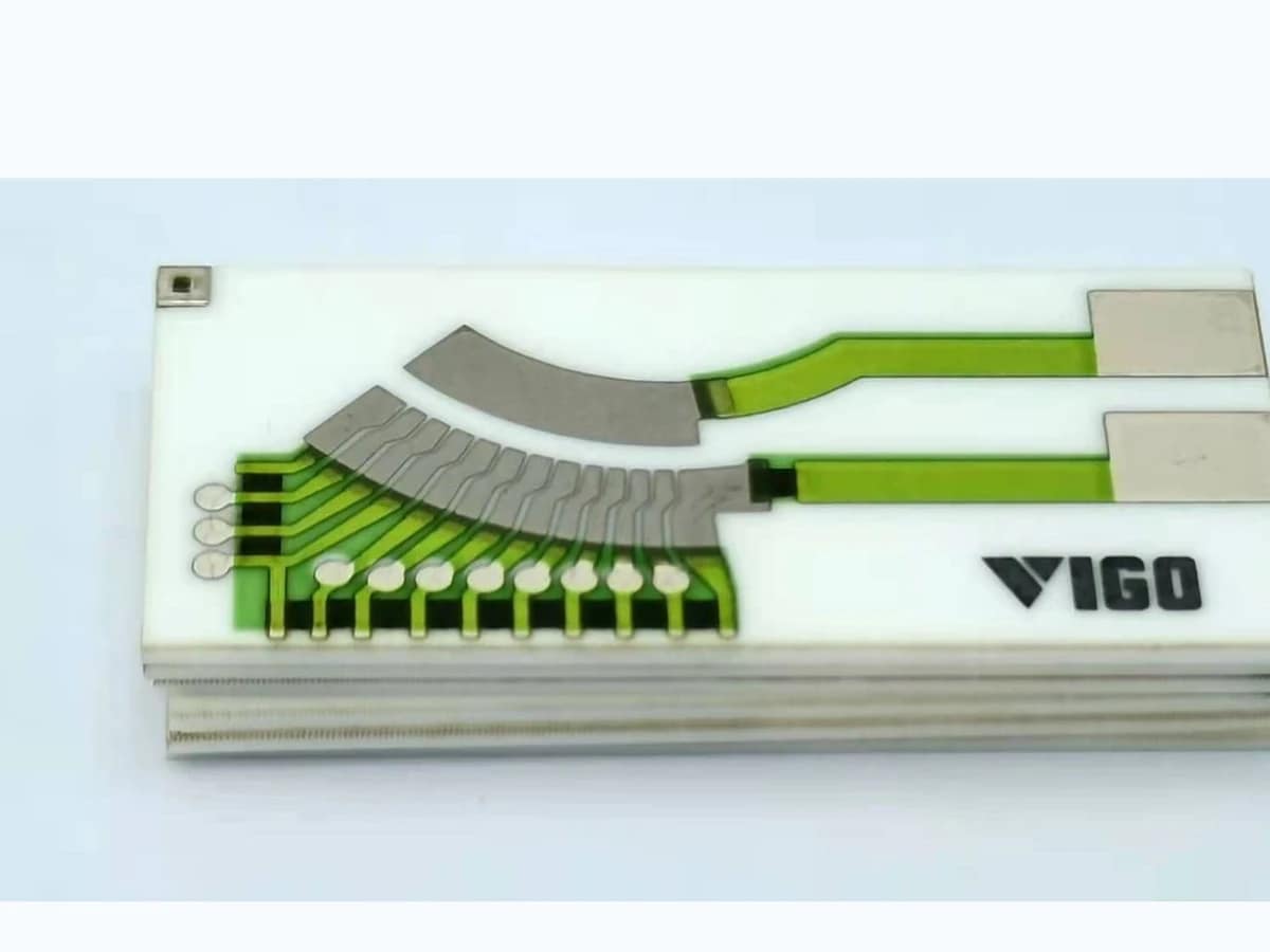
Sensing-function definition
Define the measured quantity, motion transfer, active range, output curve, resolution needs, inactive zones, channel count, and electrical interface before choosing the pattern.

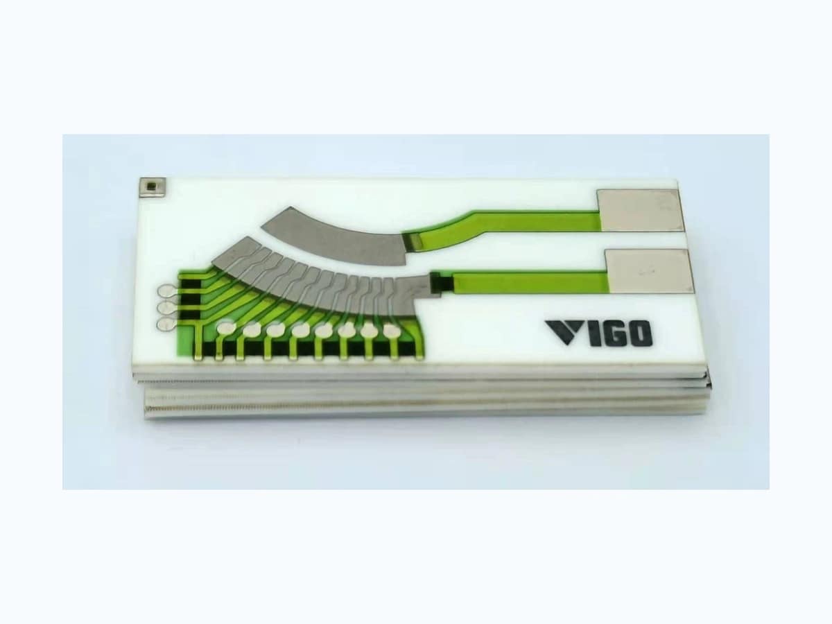
Drawing-defined resistive sensing element
A custom resistive sensor element can be shaped around a project-specific motion, level, or interface requirement when the mechanical transfer, printed geometry, resistance behavior, contact system, electronics, and environment are defined together. Chipsimple supports the drawing, material-route, prototype, and validation review.
Verified capability review
Custom Resistive Sensor Element is shown against approved company capability control sheets.
Capability source: approved company category control sheets. Final values remain drawing- and sample-controlled.
| Parameter | Standard capability | Engineering review range | Final release |
|---|---|---|---|
| Sensing function | Measured variable, motion transfer, active range, direction, endpoints, and required output are defined by the application | Rotary, linear, arc, level, pedal, valve, or custom geometry is selected only after the complete mechanism is known | Released mechanism drawing, electrical table, approved sample, and validation plan |
| Output definition | Resistance or voltage table, curve type, tolerance, loading, track count, and calibration are drawing-controlled | Linearity, taper, segmentation, redundancy, correlation, diagnostics, and measurement method are reviewed by function | Released mechanism drawing, electrical table, approved sample, and validation plan |
| Contact and environment | Mating contact, force, speed, support, terminals, media, temperature, contamination, and enclosure are project-selected | Wear, intermittent output, drift, misalignment, corrosion, leakage or isolation, and connector faults define the risk plan | Released mechanism drawing, electrical table, approved sample, and validation plan |
| Validation method | The production-intent mechanism, contact, electronics, environment, motion profile, and calibration fixture control acceptance | Sample size, stress sequence, failure limits, reporting, traceability, and end-of-line checks are agreed before release | Released mechanism drawing, electrical table, approved sample, and validation plan |
| Parameter | Standard capability | Engineering review range | Final release |
|---|---|---|---|
| Substrate Material | Alumina / FR-4 / PI approved routes | Select alumina, FR-4, or PI from stiffness, contact support, media, temperature, mounting, and cure/firing needs | Approved material specification, drawing, and incoming criteria |
| Sensor Geometry | Rotary / Linear / Arc | Travel angle or distance, active arc, datum, dead zones, endpoints, and contact path by mechanism drawing | Released drawing, DFM approval, and first-article inspection |
| Resistor System | RuO₂ / Carbon | RuO₂ or carbon selected for substrate, curve, contact load, environment, and electrical loading | Released drawing and approved sample |
| Conductor System | Ag / Ag-Pd / Au / Ag-C | Ag, Ag-Pd, Au, or Ag-C selected for terminal, wiper, media, corrosion, and process compatibility | Approved material stack, assembly interface, and sample |
| Track Count | 1–4 tracks typical | Within 1–4 tracks, redundancy, diagnostics, isolation, and terminal count follow the system schematic | Released drawing, DFM approval, and first-article inspection |
| Nominal Resistance | 100 Ω–1 MΩ typical | Within 100 Ω–1 MΩ, endpoints, intermediate points, ratios, and loading follow the approved curve table | Released electrical limits, measurement method, and approved sample |
| Resistance Curve | Linear / Nonlinear / Segmented | Linear, nonlinear, segmented, or customer point table with defined scan direction and reference condition | Released electrical limits, measurement method, and approved sample |
| Resistance Tolerance | ±1–10% by material system | Within ±1–10%, limits are allocated by material system, measurement position, fixture, and electronics | Released electrical limits, measurement method, and approved sample |
| Linearity | ±0.5–2% FS typical | Within ±0.5–2% FS typical, define best-fit or terminal-based calculation, usable travel, and hysteresis | Released electrical limits, measurement method, and approved sample |
| TCR | ±100–200 ppm/°C ceramic reference | ±100–200 ppm/°C ceramic reference; final TCR range, tracking, and temperature points follow the selected paste system | Released electrical limits, measurement method, and approved sample |
| Contact System | Precious metal / Carbon | Precious-metal or carbon contact with defined geometry, force, speed, current, lubricant, and contact path | Approved material stack, assembly interface, and sample |
| Operating Temperature | -40 to +125°C, system-dependent | -40 to +125°C category envelope is checked with media, vibration, humidity, electrical load, and mating materials | Approved electrical-thermal design and instrumented prototype validation |
| Life-test conditions | Full-travel cycling is defined with speed, stroke, direction, contact force, electrical load, and starting condition | Cycle count, media, temperature, vibration, contact noise, curve drift, wear, and endpoint limits by mechanism risk | Approved mating contact, lifecycle profile, and validation report |
A useful custom review converts the sensing problem into controlled geometry, materials, interfaces, and test criteria. The element is not released from a product name alone; it is released from the complete measurement chain.
Define the measured quantity, motion transfer, active range, output curve, resolution needs, inactive zones, channel count, and electrical interface before choosing the pattern.
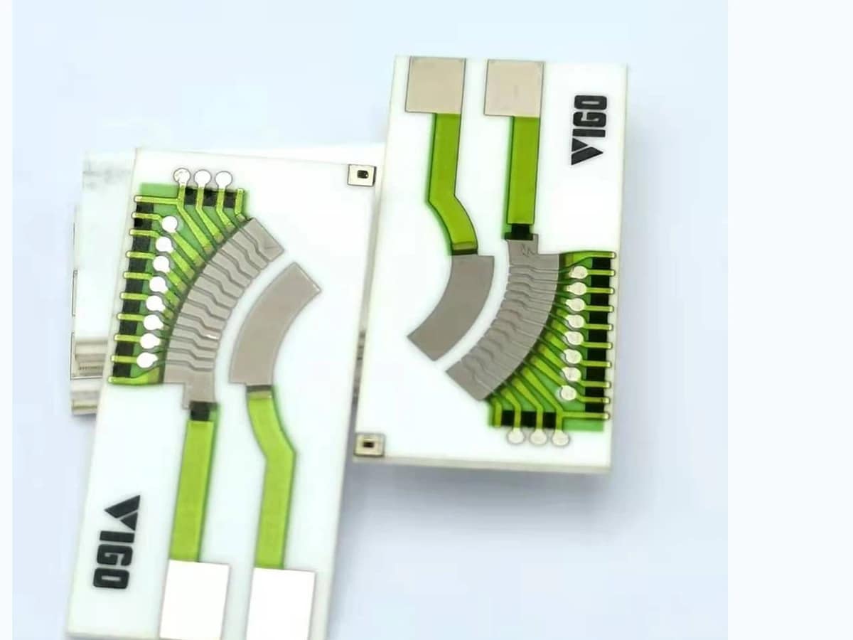
Select alumina, FR-4, or PI and a compatible resistor, conductor, pad, and overlap system against geometry, assembly, environment, and validation needs.
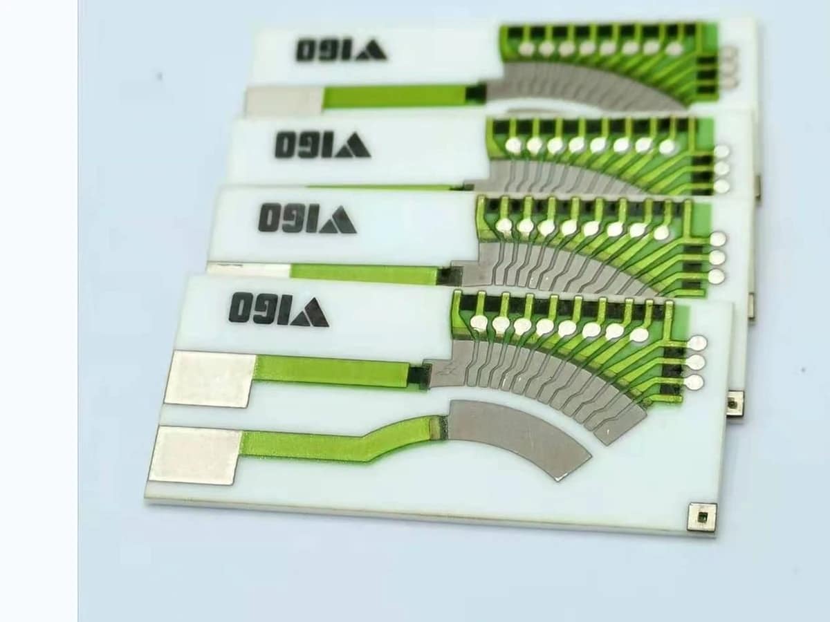
Review support, mounting, datum scheme, wiper or contact material, force, speed, path, terminals, connector, enclosure, and tolerance stack as one interface.
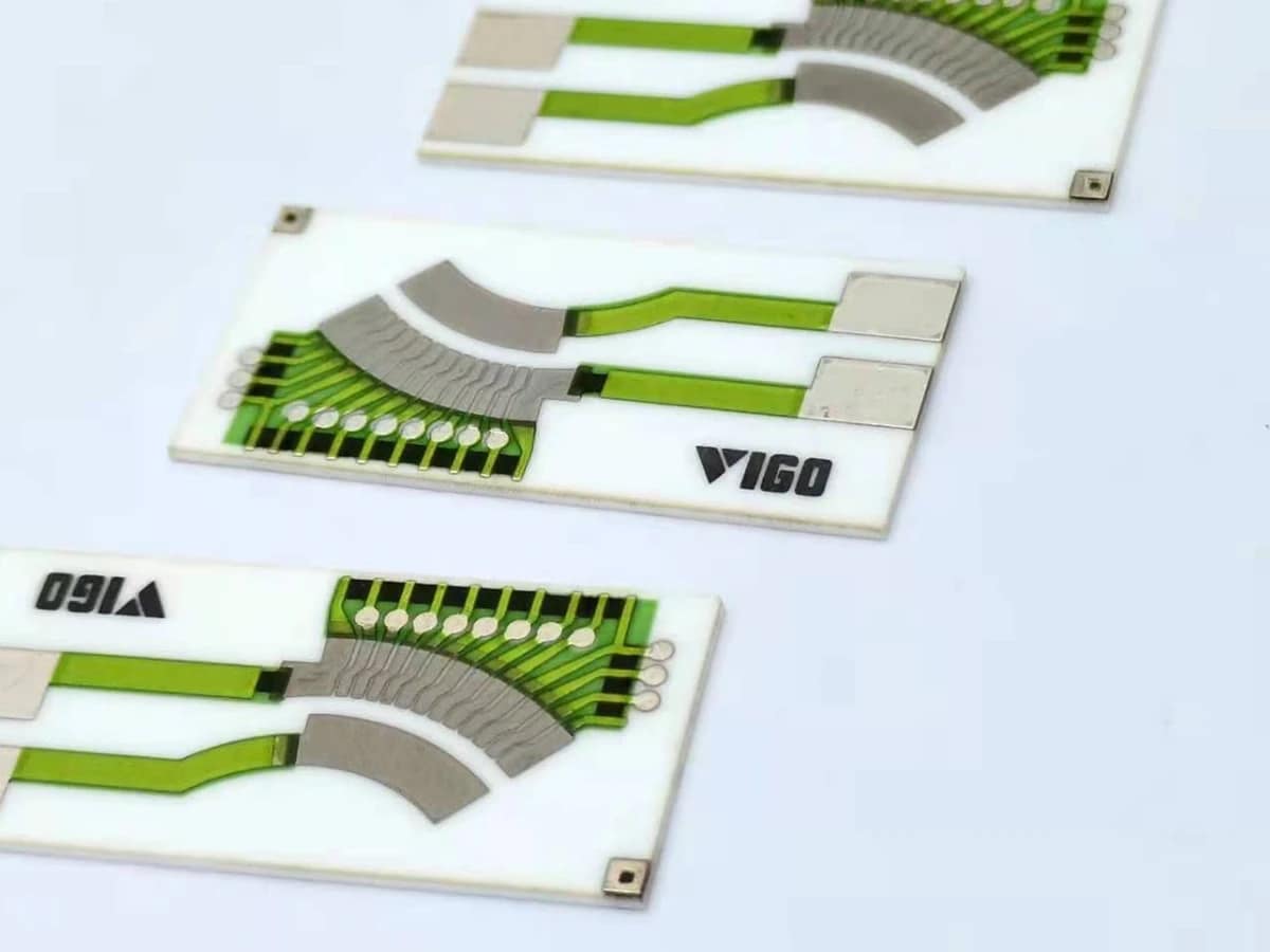
Release drawing-defined dimensional, resistance, curve, linearity, contact, environmental, lifecycle, and calibration checks with the prototype and production plan.
Custom elements may support several sensing directions, but each requires its own mechanics, electronics, contact system, environment, and validation program.
Application images are engineering illustrations, not customer projects, production records, or evidence of a released design. Suitability is confirmed only after the drawing, interfaces, operating conditions, risks, and validation plan are reviewed.
 Application illustration
Custom elements may fit joints, actuators, or slides after travel, speed, support, contact force, output curve, controller loading, duty, and calibration are defined.
Review application inputs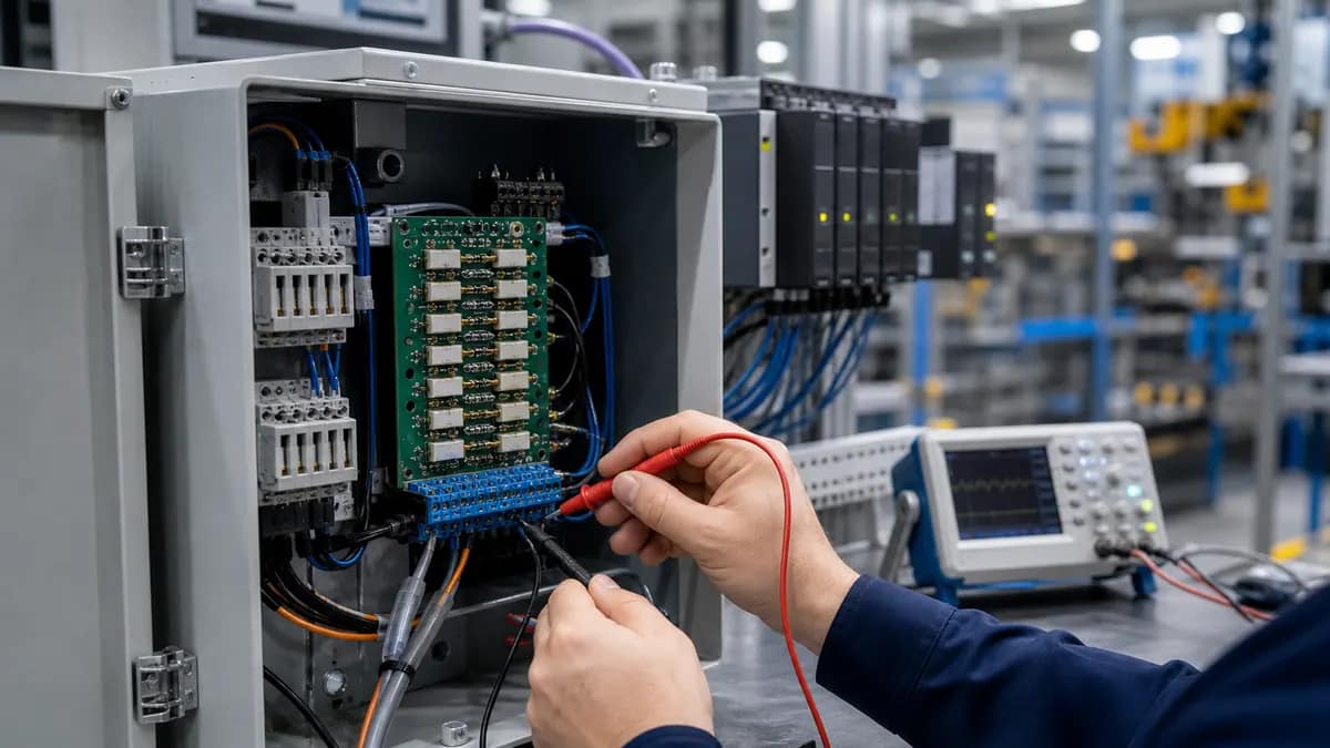 Application illustration
Industrial modules require controlled mounting, enclosure, terminals, loading, temperature, contamination, signal conditioning, inspection, and field-duty validation.
Review application inputs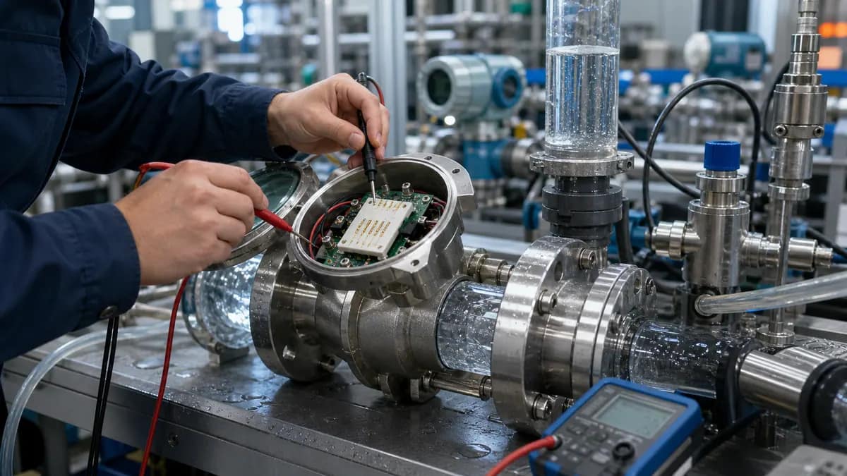 Application illustration
Process instruments can be evaluated only after the measured variable, mechanical transfer, media isolation, electrical response, calibration, and environmental limits are released.
Review application inputsVerified photographs show complete white rectangular elements with visible arc-shaped printed regions, conductor routing, terminals, and sample markings. Surface appearance alone does not identify the material system or establish electrical and reliability performance.
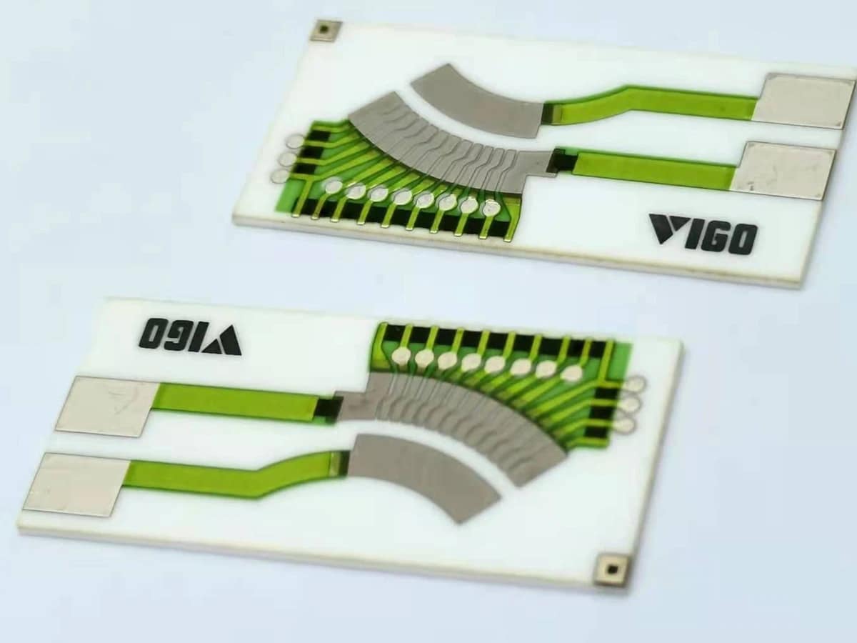
Chipsimple supports drawing-led printed sensor elements with controlled printing, resistance adjustment where applicable, dimensional and electrical inspection, and protected handling.
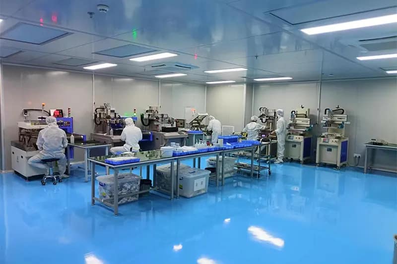
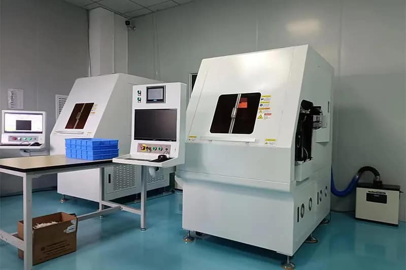
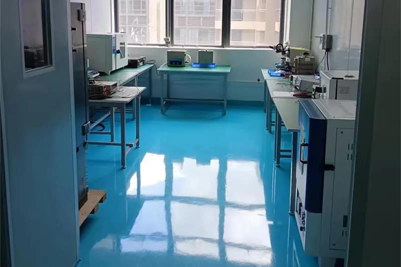
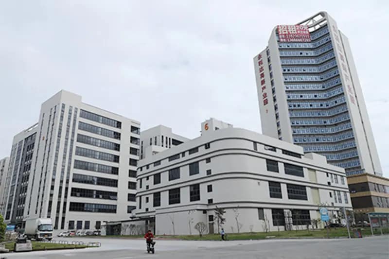
The exact route depends on substrate, resistor system, contact design, and validation plan; these photographs show general company capability, not evidence of the displayed product batch.
Short answers for quotation planning; released drawings and validation requirements remain controlling.
Begin with the measured variable, motion or interface, active range, available envelope, output curve, channel count, electrical loading, contact mechanics, mounting, terminals, environment, lifecycle target, calibration, and acceptance method. These inputs determine the appropriate substrate and printed-system route.
No. These are category-level selection values, not a released part specification. Substrate, resistor and conductor systems, geometry, resistance, tolerance, linearity, TCR, contact route, and operating temperature are narrowed against the drawing, mating mechanics, electronics, and validation plan.
Validate the element with production-intent mechanics, contacts, electronics, support, and enclosure. Check the complete output across travel, repeatability, hysteresis, contact stability, loading, environment, cycling, calibration, and inspection correlation against released limits.
Send the controlled drawing or artwork, dimensions and tolerances, active travel or angle, resistance and output-curve data, track count, mating contact, electrical loading, environment, validation method, quantity, and schedule. If the concept is new, include a system sketch and measurement chain showing how the input variable reaches the sensing surface and how the signal is conditioned.
Share the sensing objective, mechanism, envelope, output curve, contact concept, electronics, environment, and acceptance targets. We will convert the brief into DFM questions and a controlled prototype route.
PDF, DWG, DXF, STEP, Gerber, ZIP, Excel, Word, or sample photos are accepted.
The drawing-upload form loads as you reach this section.