PI Flexible Thick Film Circuit
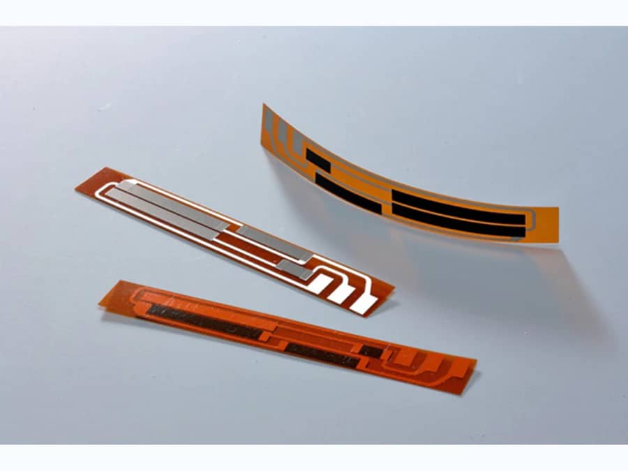
Flexible polyimide film circuit with printed resistor, heater, or sensor patterns for compact assemblies.
View Details

Custom Thick Film Circuit Manufacturer
Chipsimple manufactures ceramic thick film circuits, printed resistors, heater plates, fuel level sensor cards, and throttle position resistor circuits with controlled printing, firing, laser trimming, and inspection.
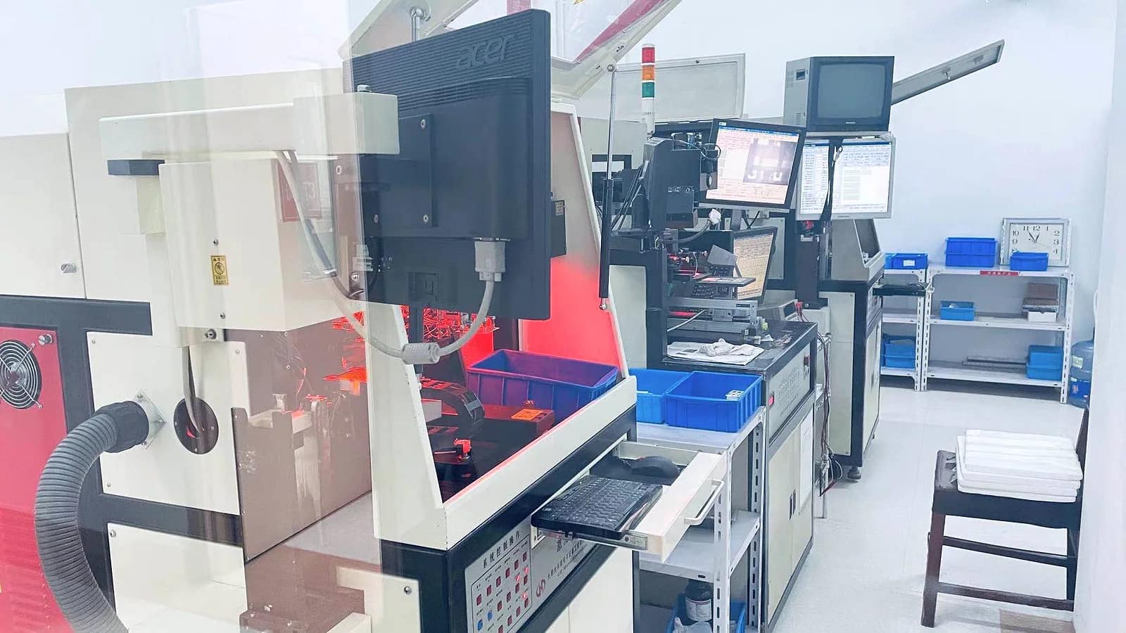
The RFQ stage is used to confirm substrate, paste system, resistance target, thermal load, sensor curve, terminals, and inspection method before production tooling.
We support alumina, aluminum nitride, stainless steel, aluminum, PI, and FR4 routes for custom thick film PCB, hybrid circuit substrates, resistor networks, and heating elements.
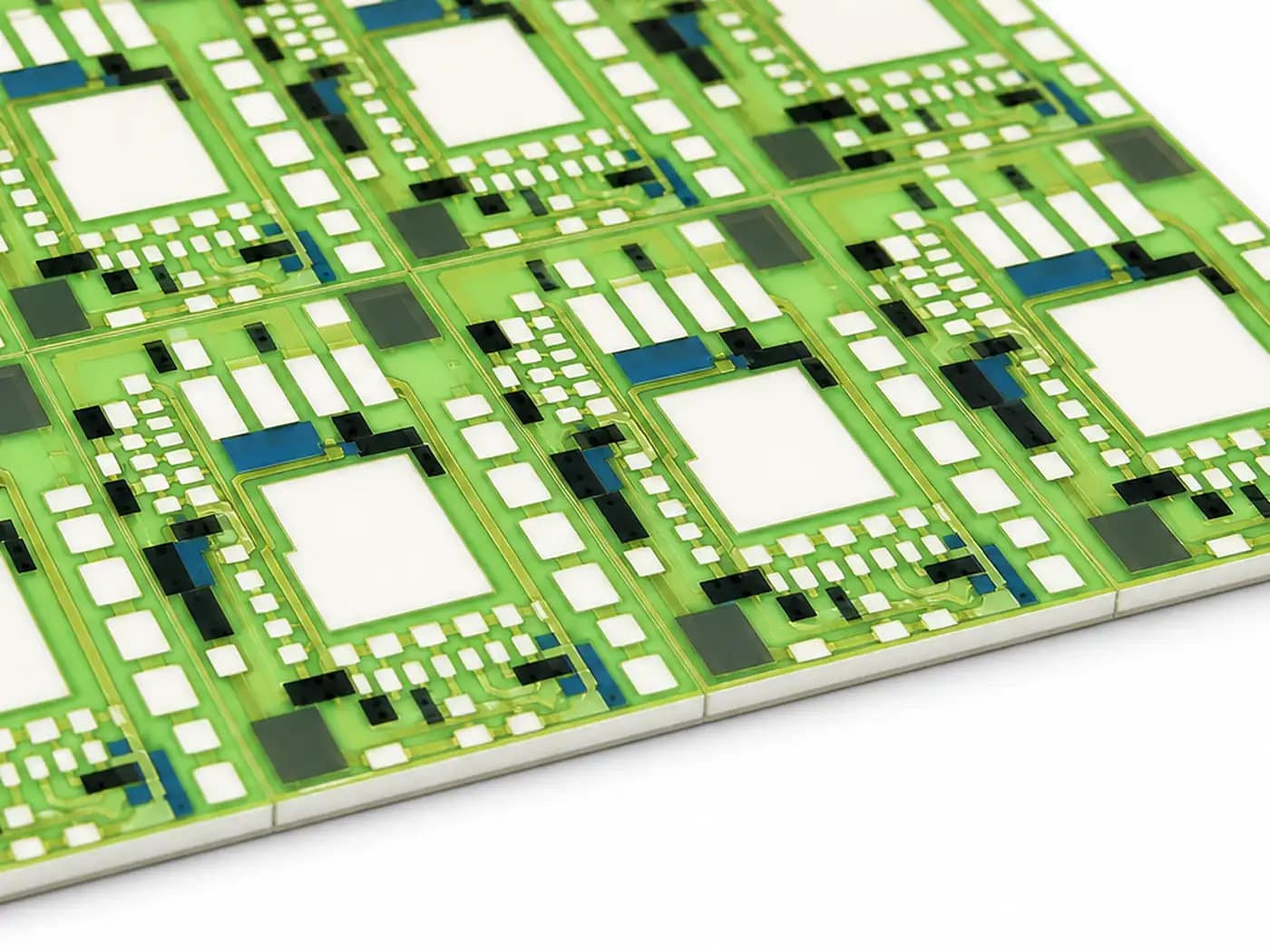
Flexible polyimide film circuit with printed resistor, heater, or sensor patterns for compact assemblies.
View Details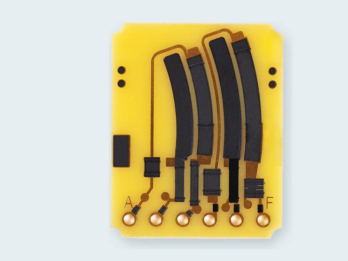
Drawing-controlled FR4 boards with printed resistor tracks, conductor interfaces, target curves, and contact zones.
View Details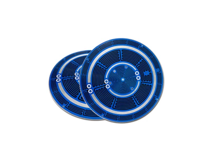
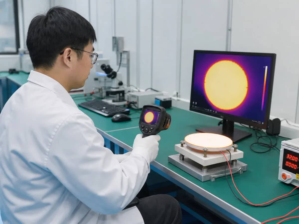
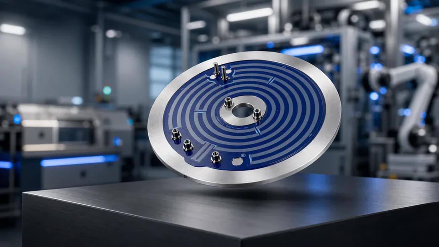
Stainless steel heater plate with dielectric layer and printed thick film heating track for thermal modules.
View Details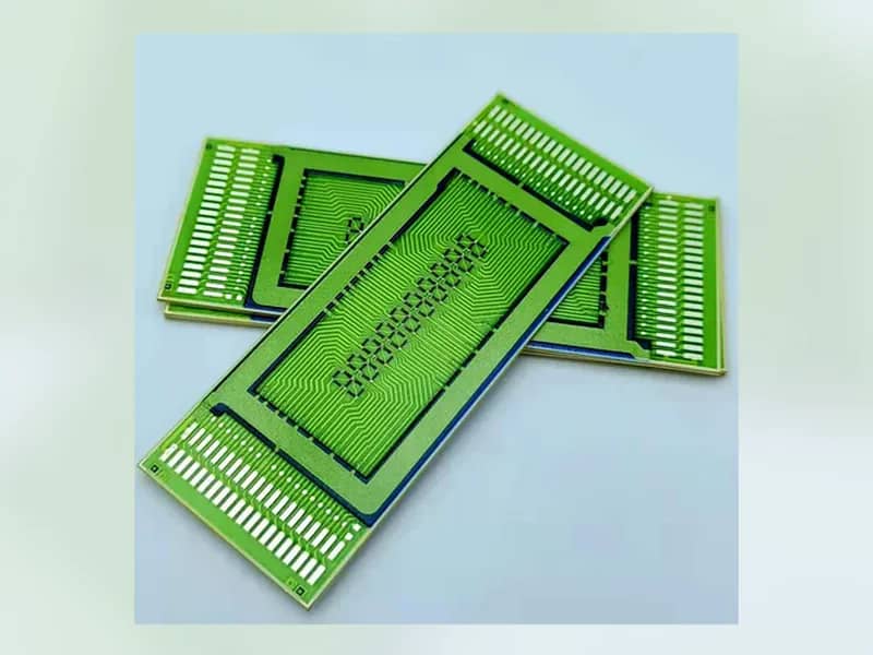
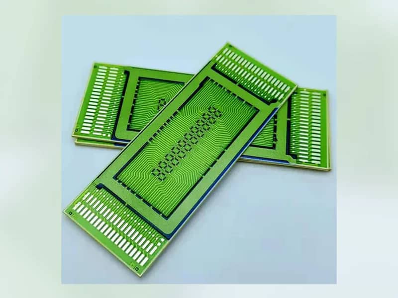
Custom alumina ceramic substrates with conductor, resistor, dielectric, and interface features reviewed by drawing.
View DetailsThick film ceramic circuits are selected when compact size, thermal stability, resistance accuracy, and harsh-environment reliability matter.
Product and company photographs are shown as route references. Application suitability remains controlled by the drawing and operating conditions.
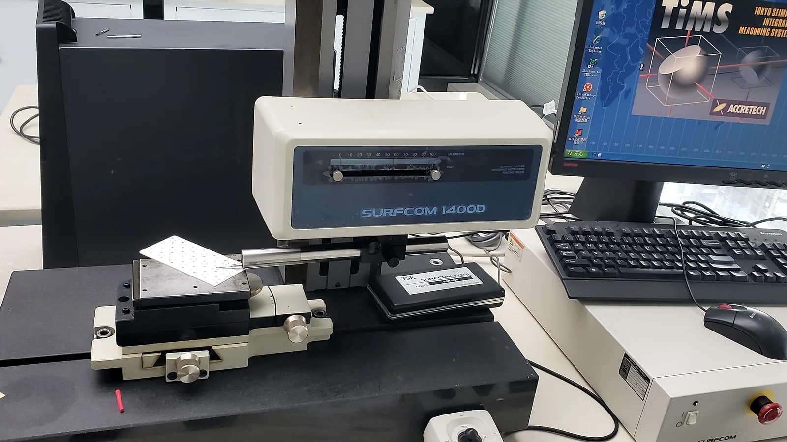
Review screen accuracy, paste compatibility, drying, firing profile, and fired layer stability before batch release.
Define resistance tolerance, curve targets, active or passive trimming method, and measurement points for repeatability.
Check solder pads, lead or harness connection, SMT or module interface requirements, coating, and mechanical stress.
Align visual inspection, dimensional check, resistance test, insulation test, aging, packaging, and lot traceability.
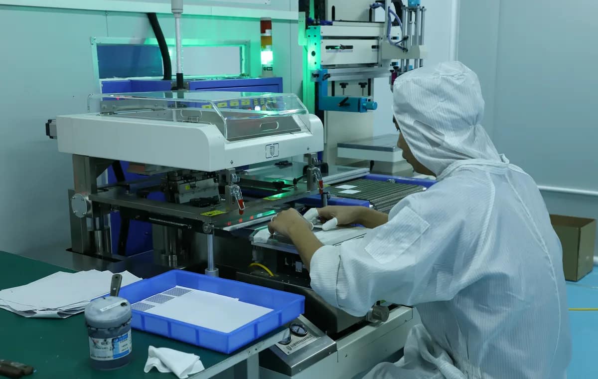
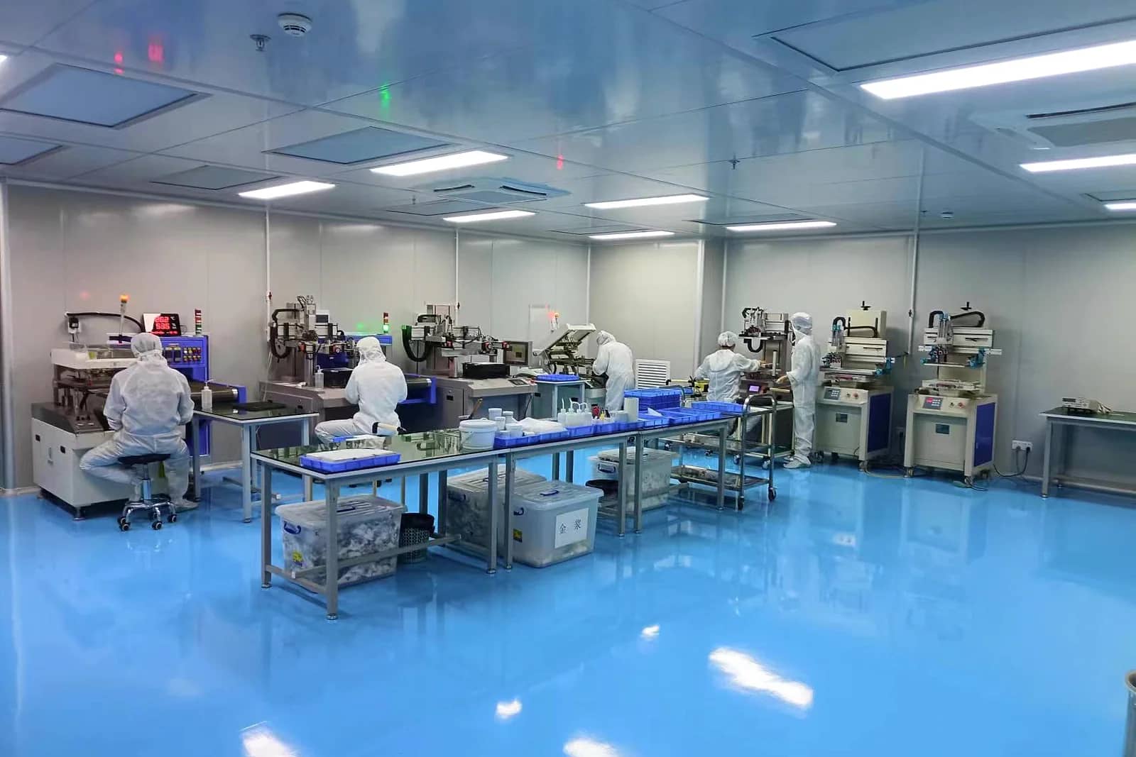
Include substrate, size, resistance, voltage, power, tolerance, quantity, and test requirements.
Request a Quote