Film and printed stack
Select the substrate and printed conductor, resistor, dielectric, or protective layers as a compatible system. Thickness, cure sequence, adhesion, and exposed contact windows are confirmed before the artwork is frozen.

Flexible printed functional circuit
Custom polymer thick film circuits combine a flexible film substrate with printed conductor, resistor, or contact functions in a drawing-led format. Chipsimple reviews the material, printed stack, termination, bend condition, electrical target, assembly interface, and validation method together before prototyping or repeat production.
Verified capability review
Custom Polymer Thick Film Circuit is shown against approved company capability control sheets.
Capability source: approved company category control sheets. Final values remain drawing- and sample-controlled.
| Parameter | Standard capability | Engineering review range | Final release |
|---|---|---|---|
| Substrate Material | PI / PET / PEN / Polycarbonate | PI, PET, PEN, or polycarbonate selected for temperature, flex, chemistry, stiffness, and cure compatibility | Approved material specification, drawing, and incoming criteria |
| Substrate Thickness | 25–250 µm typical | Within 25–250 µm, handling, stiffness, connector, bend strain, and dimensional stability are reviewed | Approved material specification, drawing, and incoming criteria |
| Conductor System | Ag / Ag-C / Carbon | Ag, Ag-C, or carbon selected for current, resistance, flex, contact, and termination | Approved material stack, assembly interface, and sample |
| Resistor System | Carbon / Ag-C / PTC | Carbon, Ag-C, or PTC route by resistance function, temperature response, flex, and cure | Released drawing and approved sample |
| Printed Film Thickness | 8–12 µm typical | Within 8–12 µm typical, ink rheology, screen, cure, adhesion, and resistance are controlled together | Released drawing, DFM approval, and first-article inspection |
| Cure Temperature | 120–150°C typical | Within 120–150°C typical, peak, dwell, support, and substrate shrinkage are validated | Approved material-process route and production traveler |
| Parameter | Standard capability | Engineering review range | Final release |
|---|---|---|---|
| Minimum Line/Space | ≥150 µm typical | At ≥150 µm, registration, spreading, flex zone, conductor load, and inspection access are reviewed | Released drawing, DFM approval, and first-article inspection |
| Printed Layers | 1–4 layers typical | Within 1–4 layers, alignment, interlayer compatibility, cure sequence, and neutral-axis strain are reviewed | Released drawing, DFM approval, and first-article inspection |
| Minimum Bend Radius | ≥5 × substrate thickness, static | The ≥5× thickness value is for static use; dynamic flex needs direction, cycles, speed, and strain-relief review | Agreed lifecycle profile, acceptance drift, and validation report |
| Operating Temperature | -40 to +90°C typical | The -40 to +90°C typical range is checked with humidity, fluids, enclosure, load, and bend state | Approved electrical-thermal design and instrumented prototype validation |
| Resistance Tolerance | ±5% / ±10% typical | ±5% or ±10% selected by function, geometry, ink, cure, flex state, and measurement method | Released electrical limits, measurement method, and approved sample |
| Termination | Pad / Crimp / Connector / Conductive adhesive | Pad, crimp, connector, or conductive adhesive selected with mating parts, stiffener, contact load, and assembly process | Approved material stack, assembly interface, and sample |
A manufacturable custom circuit depends on the complete interface, not only the printed artwork. Engineering review connects film selection, conductor and resistor compatibility, print registration, cure sequence, contact protection, bend direction, connector or adhesive termination, and the measurement method used for release.
Select the substrate and printed conductor, resistor, dielectric, or protective layers as a compatible system. Thickness, cure sequence, adhesion, and exposed contact windows are confirmed before the artwork is frozen.
Release line geometry, overlaps, pad arrays, keep-outs, alignment features, bend zones, and any multi-layer registration requirement in controlled artwork with a clear revision.
Define pad, crimp, connector, conductive-adhesive, stiffener, metal-backer, pressure-contact, and housing conditions so the flexible part is reviewed in its real assembly.
Resistance, continuity, contact behavior, adhesion, bend exposure, dimensional fit, environment, and lifecycle checks are selected from the actual duty rather than inferred from a photograph.
Custom film circuits fit compact products when printed electrical functions must follow an unusual outline or constrained assembly. Each application still needs its own contact, environment, movement, and validation definition.
Application images are engineering illustrations, not customer projects, production records, or evidence of a released design. Suitability is confirmed only after the drawing, interfaces, operating conditions, risks, and validation plan are reviewed.
 Application illustration
Flexible printed routing and resistive functions may fit constrained control assemblies after connector, bend, enclosure, electrical load, and service environment are defined.
Review application inputs Application illustration
Thin film circuits can support compact interfaces where material declarations, cleaning exposure, electrical limits, assembly pressure, and validation are controlled by the device program.
Review application inputs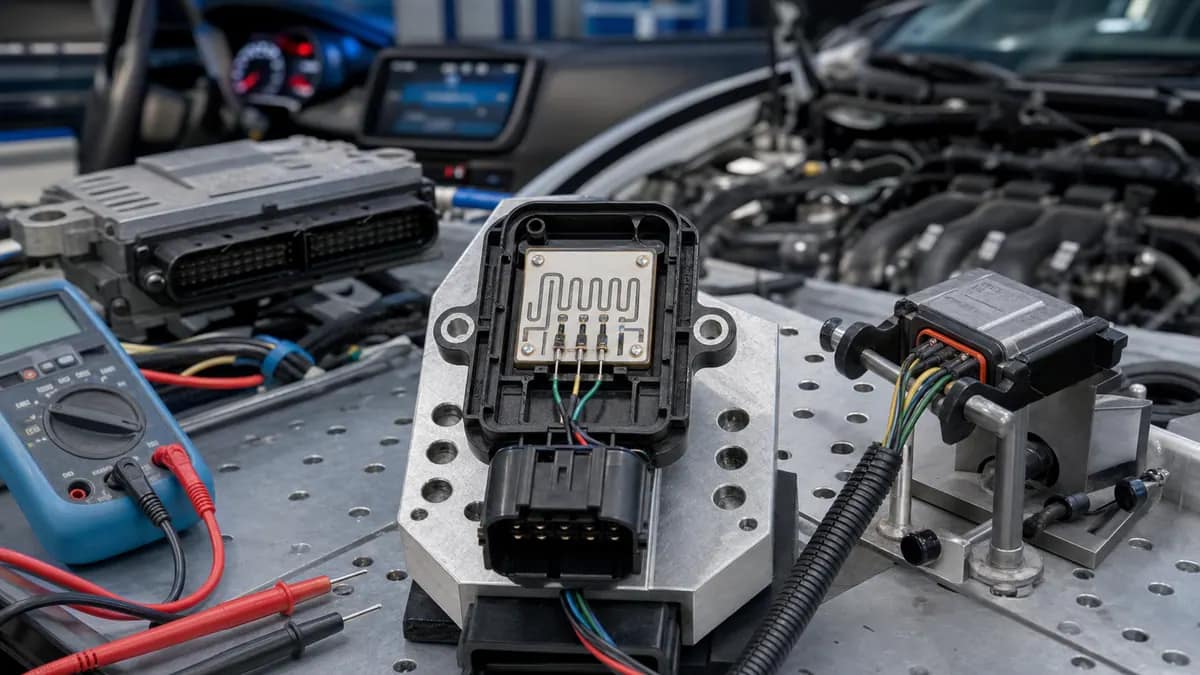 Application illustration
Custom flexible circuits may be reviewed for space-limited modules after temperature, vibration, humidity, contact mechanics, connector retention, and vehicle-level test requirements are supplied.
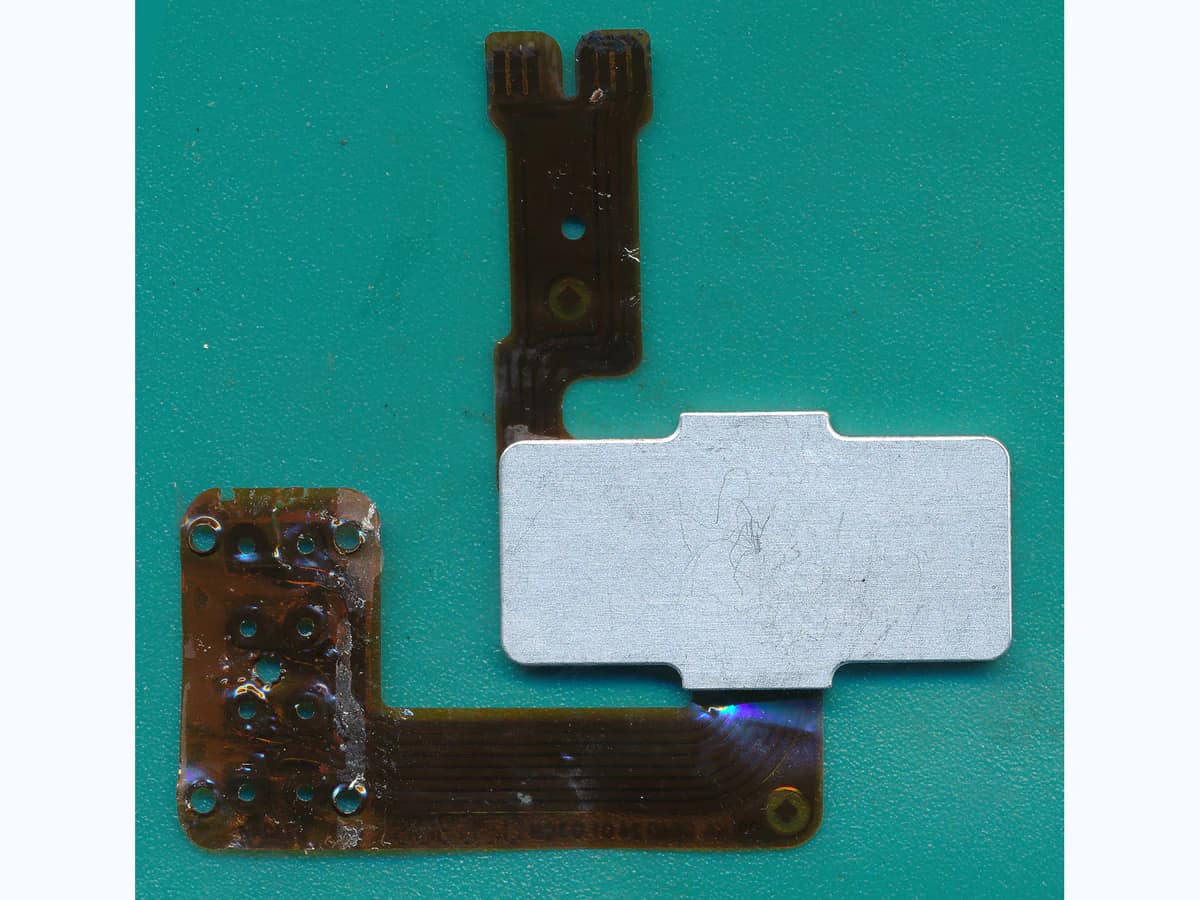
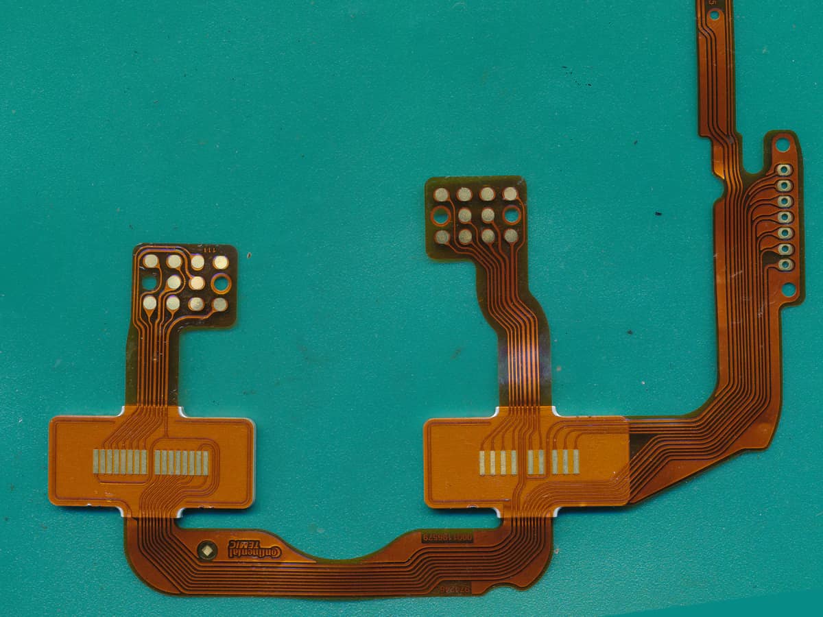
Review application inputsThe gallery and detail image show real supplied flexible circuits with varied outlines, printed paths, terminal pads, holes, and attached metal-backed areas. Surface photographs establish visible construction only; they do not establish material grade, hidden layer count, resistance, bend life, adhesion, or environmental performance.
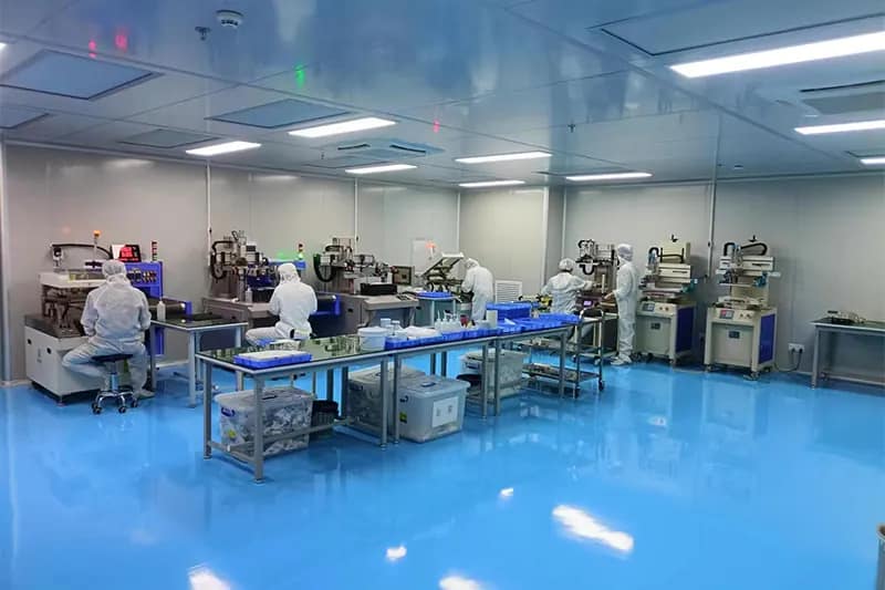
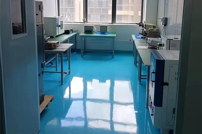
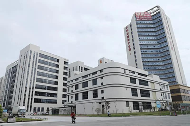
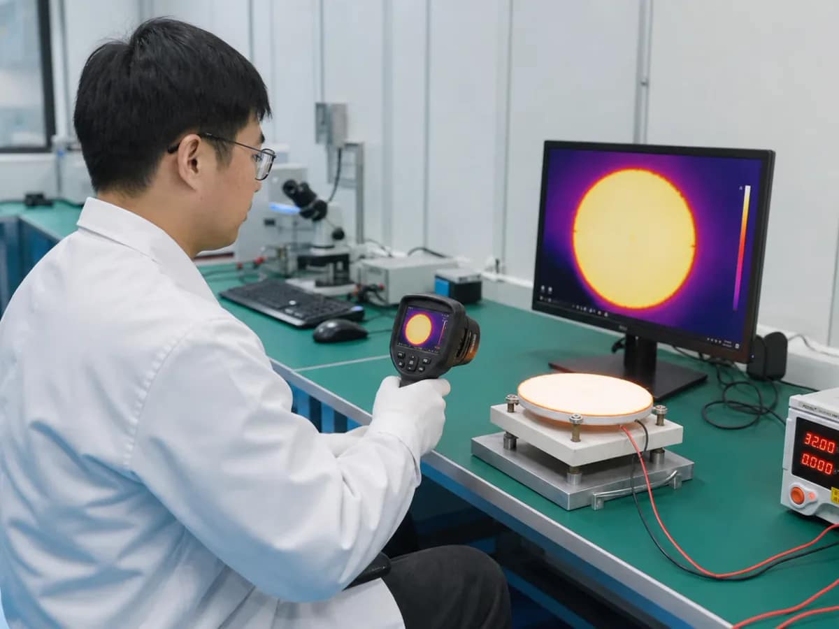
Chipsimple supports controlled printing, laboratory inspection, production management, and protected packing in Dongguan.
For each polymer circuit, the approved film, printed material set, artwork revision, cure route, termination, inspection method, sampling, and acceptance records are confirmed before repeat production; project capability remains subject to engineering review.
Short answers for quotation planning; released drawings and validation requirements remain controlling.
Start with the film material and thickness, circuit outline, printed layer artwork, conductor and resistor function, contact windows, bend direction and radius, termination, stiffener or backing, assembly method, electrical targets, environment, and validation plan. These inputs determine whether the proposed material stack and process route are suitable.
No. They are practical category-level selection values, not a released product specification. Material compatibility, geometry, print build, electrical loading, assembly, environment, inspection method, and expected volume can narrow the usable window. Final values are confirmed against the controlled drawing and approved project conditions.
Validate the released dimensions and fit first, then continuity, resistance or functional response, contact interface, adhesion, and any project-selected bend, humidity, temperature, chemical, or lifecycle exposure. The test method, sample size, conditioning, electrical loading, and acceptance limits must be defined before results are treated as a product rating.
Send the controlled drawing or artwork, dimensions and tolerances, material preference, electrical targets, assembly interface, operating environment, validation requirements, prototype quantity, annual volume, and schedule. Include the bend zone, connector or adhesive interface, contact exposure, backing or stiffener details, and any dynamic-flex duty.
Send the controlled artwork and real assembly conditions so the film, printed stack, termination, bend zones, electrical targets, and validation route can be reviewed together. Clear revision control and measurable acceptance limits reduce avoidable prototype loops and make repeat-production planning more reliable.
PDF, DWG, DXF, STEP, Gerber, ZIP, Excel, Word, or sample photos are accepted.
The drawing-upload form loads as you reach this section.