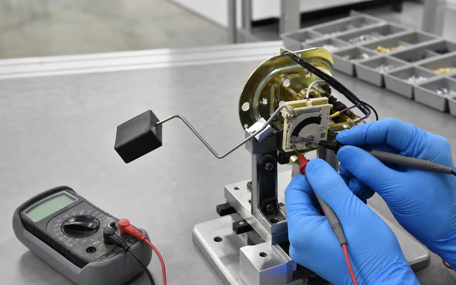
Automotive sensing
Position, level, throttle, oil, and related sensor projects connect track geometry, wiper contact, output curve, wear, media exposure, and end-of-line calibration.
Read the sensor guide
Thick Film Technology Center
Engineering guidance for materials, printing, thermal processing, resistor design, inspection, and RFQ planning.
Use this center to select the right circuit route, identify design inputs, understand process controls, and prepare a manufacturable thick film project.
Technical review: Chipsimple Engineering Team. Company-source process evidence, published technical references, and drawing-controlled manufacturing requirements; scope includes ceramic thick film circuits, printed resistors, sensor circuits, and thick film heaters.
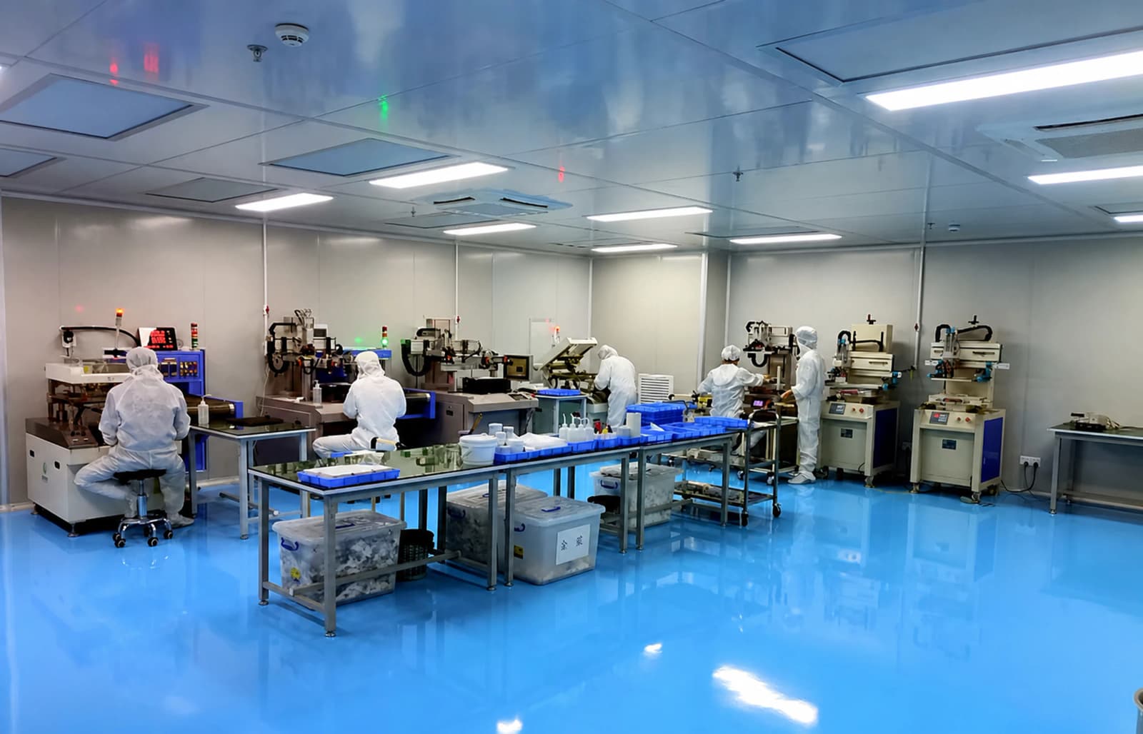
A thick film circuit is a printed functional system. The correct route depends on what the circuit must sense, heat, resist, interconnect, insulate, or survive after assembly.
Functional pastes are deposited on a compatible substrate and processed to form controlled electrical layers. Unlike an ordinary interconnect-only PCB, the printed stack can become part of the sensing, resistance, heating, insulation, or hybrid-assembly function.
The substrate property alone does not define the finished circuit. Paste chemistry, geometry, firing or curing, refire sequence, termination, trimming, assembly, and validation work as one system.
These ceramic and printed-circuit technologies are related, but they are not interchangeable.
| Route | How the circuit is formed | When to evaluate it |
|---|---|---|
| Thick film | Functional conductor, resistor, dielectric, protective, or heater pastes are printed and thermally processed on a compatible substrate. | Integrated resistors, sensor tracks, heaters, ceramic hybrids, and application-specific functional circuits. |
| Thin film | Vacuum-deposited films are patterned with photolithographic processes. | Fine geometry, precision networks, and applications where deposited-film control is the main requirement. |
| DPC | Copper is deposited and plated on ceramic, then patterned as the interconnect system. | Dense ceramic interconnect and thermal designs that need a plated-copper route rather than printed functional pastes. |
| DBC or AMB | Copper foil is bonded to a ceramic substrate through a route selected for the ceramic and assembly. | Power electronics where copper thickness, current handling, and the thermal path dominate the architecture. |
Substrate, conductor, resistor, dielectric, protection, terminal, and assembly materials must survive the same process sequence and operating environment.
Engineering boundary: final materials and capability are confirmed against the released drawing, selected paste system, assembly route, and validation method.
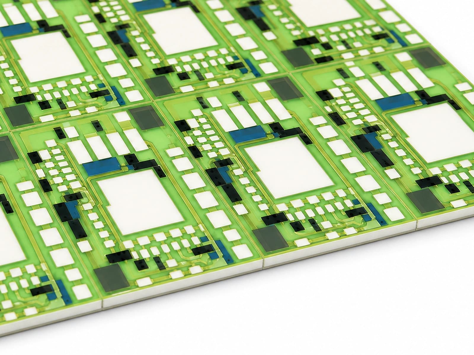
Process control is sequential. A change in paste, screen, drying, firing, trim geometry, or test method can change the final electrical result.
Function, drawing, materials, assembly, environment, test method, and volume are aligned before artwork release.
Material, surface condition, outline, holes, slots, and cleanliness are checked for the selected route.
Each functional layer uses controlled artwork, screen, paste, alignment, deposition, and drying conditions.
Compatible layers follow their released firing or curing profile, sequence, and refire limits.
Resistance values or curves can be laser trimmed where the design provides suitable geometry and measurement access.
Visual, dimensional, electrical, environmental, and documentation checks follow drawing risk and the agreed control plan.
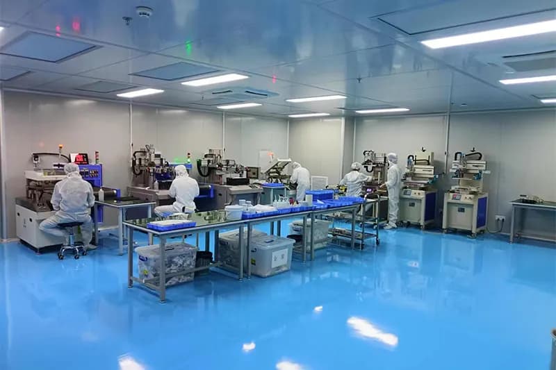
Workshop records connect the process sequence to screen printing, controlled thermal processing, and laser trimming.
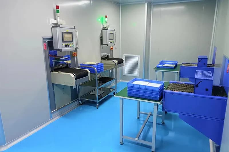
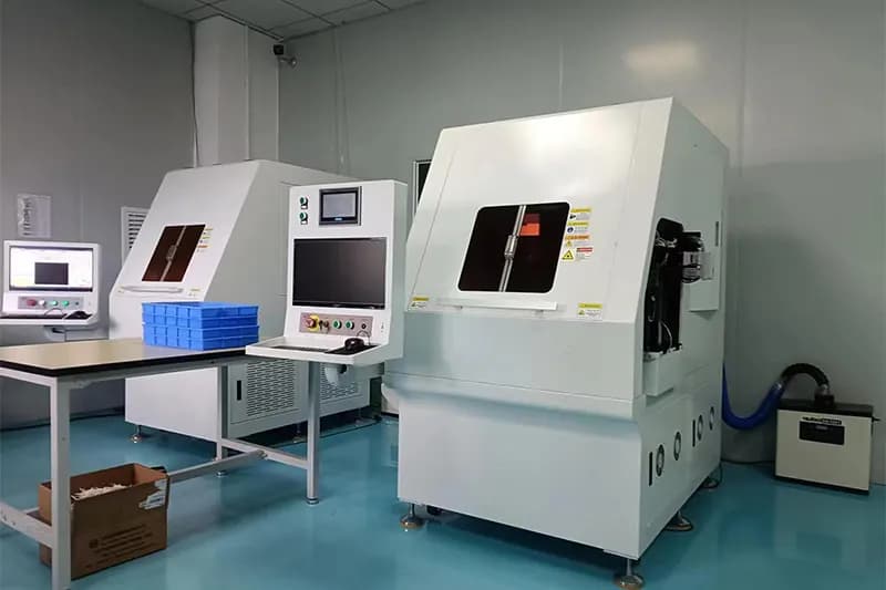
A usable RFQ describes the finished assembly and operating condition, not only the bare circuit outline.
The control plan follows the drawing, measurement method, operating risk, and approval stage. A visual pass cannot replace the required electrical or environmental result.
Coverage, alignment, edge condition, overlap, pinholes, contamination, and pad condition
Outline, thickness, holes, slots, flatness, edge quality, and assembly interface
Continuity, isolation, resistance, ratio, curve, TCR, power, or dielectric checks as specified
Adhesion, solderability, humidity, thermal cycling, media exposure, wear, or aging selected by project risk
Drawing revision, lot identity, inspection results, sample approval, packaging, and shipment documents when required
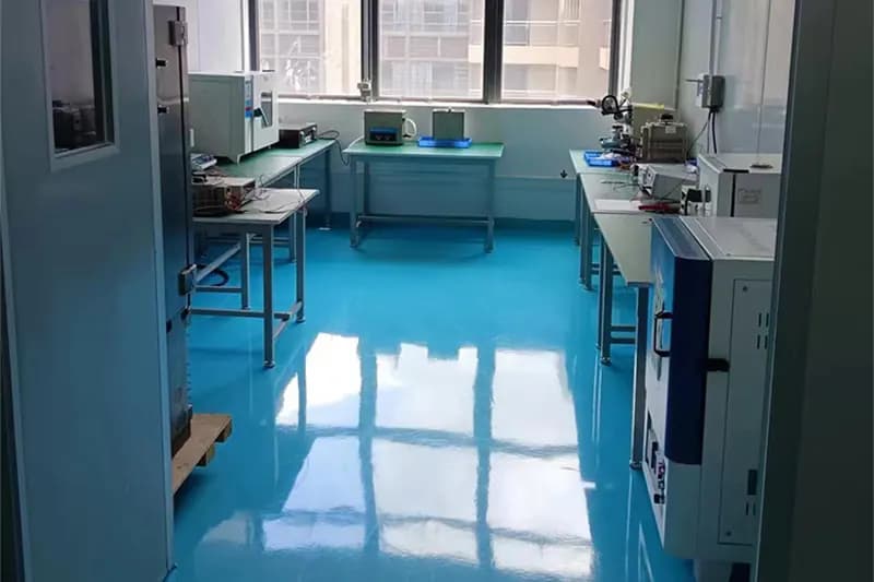
Each use case changes the required geometry, contact system, thermal path, materials, validation, and assembly interface.
Position, level, throttle, oil, and related sensor projects connect track geometry, wiper contact, output curve, wear, media exposure, and end-of-line calibration.
Read the sensor guide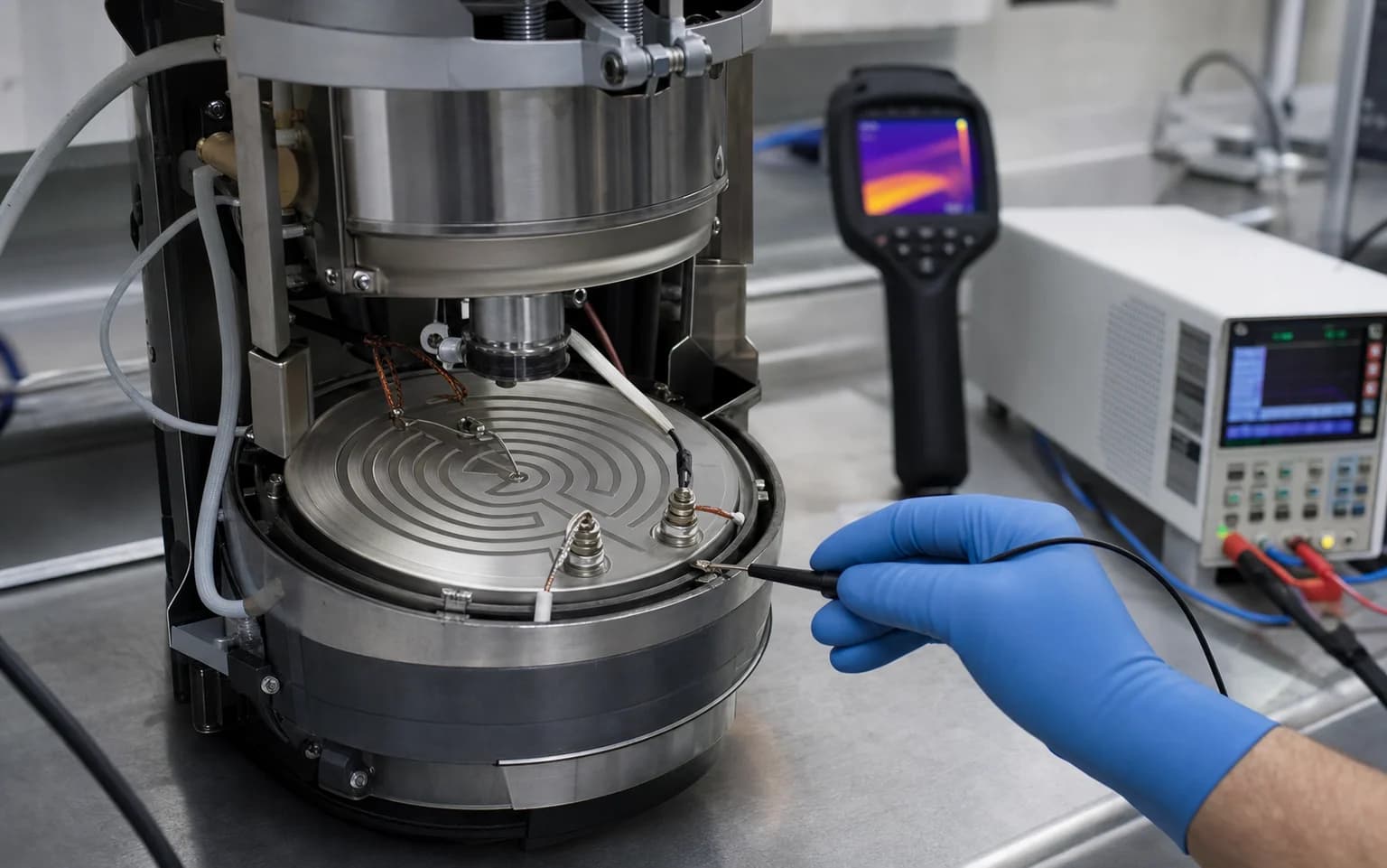
Voltage, power, heat path, insulation, sensing, flow conditions, terminals, and safety targets are reviewed at assembly level.
Explore heater engineering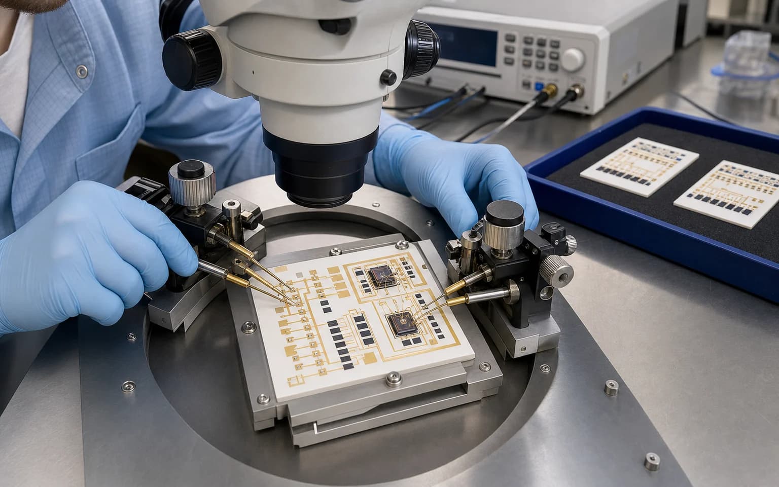
Printed resistors, conductor pads, die attach, wire bonding, protection, thermal behavior, and inspection access must share one released layout.
Review hybrid interfacesStart with fundamentals, then move through materials and process, design and reliability, and application-specific RFQ preparation.
Fast answers for early process selection. Final values and limits follow the selected stack, geometry, assembly, and validation plan.
Open Knowledge LibraryIts functional layers are deposited as pastes, commonly by screen printing, then dried and fired or cured through a material-compatible process. Conductors, resistors, dielectrics, protective layers, and heaters can be integrated in the printed stack.
No. Ceramic describes the substrate. Thick film, thin film, DPC, DBC, AMB, and other metallization routes create different conductor structures and design rules. The required function should select the process route.
Alumina is a common, established thick-film platform. AlN is evaluated when the thermal path is more demanding. The final choice also depends on paste compatibility, metallization, mechanical details, assembly, reliability, availability, and cost.
Yes, subject to engineering review. Paste family, geometry, contact design, trim allowance, probe method, operating environment, and validation plan all influence achievable value, curve, tolerance, TCR, and stability.
Send Gerber, DXF, DWG, PDF, STEP, BOM, sample photos, substrate details, electrical targets, operating conditions, assembly method, test requirements, prototype quantity, and expected annual volume when available.
Send the drawing, electrical target, material preference, operating condition, assembly method, test requirements, and quantity. If information is incomplete, clear sample photos and measured dimensions can still start the review.
Drawing revision, sample photos, BOM, or existing failure information
Resistance, curve, heating, insulation, interconnect, or sensor requirements
Temperature, media, cycling, wear, volume, and approval needs
PDF, DWG, DXF, STEP, ZIP, Excel, Word, and measured sample photos are accepted.
The drawing-upload form loads as you reach this section.