Material-stack compatibility
Review alumina grade and surface with conductor, resistor, dielectric, protection, terminal, cleaning, joining, and refire requirements before materials are released.

Alumina Ceramic Circuit Engineering
Custom alumina thick film PCBs can combine printed conductors, resistors, dielectric layers, protection, and assembly interfaces on a rigid ceramic substrate. Send the drawing, material requirement, artwork, electrical targets, operating conditions, joining method, quantity, and inspection plan so engineering can review the complete manufacturing route.
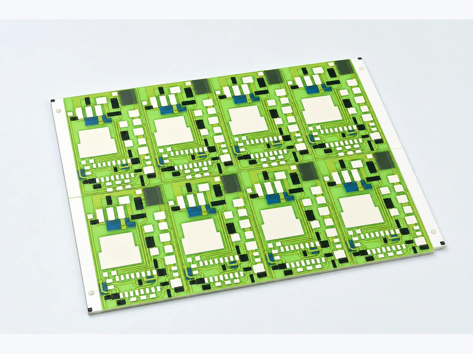
Custom alumina substrates carrying printed circuit functions. The real panel photographs show an example construction; the supplied drawing determines the delivered outline, circuit pattern and inspection requirements.
Send dimensioned artwork, alumina grade if fixed, printed-layer requirements, terminals, resistance targets, environment, test criteria and quantities.
Send DrawingsDefine the supplied alumina surface, free-state geometry and artwork datum needed for a controlled conductor-and-resistor print trial.
Compare alumina candidates using grade identity, surface response, thickness and functional acceptance rather than a purity percentage alone.
Check whether spatial sampling can hide or misrepresent periodic thick film surface features before using a smooth profile for a dimensional decision.
Verified capability review
Alumina Thick Film PCB is shown against approved company capability control sheets.
Capability source: approved company category control sheets. Final values remain drawing- and sample-controlled.
| Parameter | Standard capability | Engineering review range | Final release |
|---|---|---|---|
| Substrate Material | 96% Alumina (Al₂O₃) standard route | 99% / 99.6% alumina or AlN through material and process review | Approved material specification, drawing, and incoming criteria |
| Board Thickness | 0.25–3.0 mm | Thickness inside 0.25–3.0 mm is checked against outline, flatness, holes, handling, and firing | Approved material specification, drawing, and incoming criteria |
| Conductor System | Silver (Ag) / Silver-Palladium (Ag-Pd) | Pt-Ag, Au, bonding, soldering, contact, and high-temperature routes by compatible stack review | Approved material stack, assembly interface, and sample |
| Resistor System | RuO₂ thick film | Paste family, sheet resistance, geometry, refire sequence, and trim allowance by circuit target | Released drawing and approved sample |
| Conductor Thickness | 10–25 µm | Value inside 10–25 µm is selected for print build, firing, current path, and assembly | Released drawing, DFM approval, and first-article inspection |
| Resistor Tolerance | ±1% standard | ±0.5% available after geometry, material, trimming, and measurement review | Released drawing and approved sample |
| Parameter | Standard capability | Engineering review range | Final release |
|---|---|---|---|
| Firing Temperature | Up to 850°C | The peak profile is paste- and stack-specific within the approved route; later refires are reviewed together | Approved material-process route and production traveler |
| Thermal Conductivity | ≥24 W/m·K, 96% alumina reference | Alternative alumina grade or AlN route by approved material certificate and system thermal review | Released drawing and approved sample |
| Minimum Line/Space | ≥100 µm | Geometry at the ≥100 µm controlled capability is checked for paste, screen, registration, overlap, edge clearance, and yield | Released drawing, DFM approval, and first-article inspection |
| Board Size | Up to 120 × 120 mm | Larger than 120 × 120 mm by panel, flatness, handling, firing, and inspection review | Released drawing, DFM approval, and first-article inspection |
| Surface Finish | HASL / ENIG / ENEPIG | Finish selected for soldering, bonding, contact, storage, and downstream thermal exposure | Approved material stack, assembly interface, and sample |
| Dielectric Strength | ≥15 kV/mm | Product withstand voltage is derived from dielectric material, fired thickness, clearances, interfaces, and test method | Released insulation stack and agreed IR/withstand test plan |
Four reviews connect the ceramic, printed materials, artwork, electrical targets, and downstream assembly to one manufacturable release. Final materials, numerical limits, and records remain controlled by the customer drawing and approved project plan.
Review alumina grade and surface with conductor, resistor, dielectric, protection, terminal, cleaning, joining, and refire requirements before materials are released.
Check common datums, line and spacing rules, overlaps, openings, edge clearances, panel orientation, print direction, and inspection access across each printed layer.
Connect electrical targets, resistor or heater duty, pad finish, joining route, housing, heat path, cleaning, coating, and rework limits to the released design.
Select visual, dimensional, electrical, adhesion, assembly, traceability, and packing checks with measurable limits, sampling, equipment, and record format.
These application directions are starting points for engineering review. Suitability depends on the released electrical, thermal, mechanical, environmental, assembly, and validation requirements.
Application images are engineering illustrations, not customer projects, production records, or evidence of a released design. Suitability is confirmed only after the drawing, interfaces, operating conditions, risks, and validation plan are reviewed.
 Application illustration
Alumina circuits can be reviewed for compact resistor networks when the resistance map, tolerance, TCR, power distribution, trimming strategy, terminals, environment, and test method are drawing-defined.
Review resistor inputs Application illustration
Heater layouts require voltage, power, target temperature, heat-transfer boundary, resistance tolerance, sensor interface, mounting, insulation, cycling, and safety criteria before the printed route is selected.
Review heater inputs Application illustration
Printed tracks and terminal patterns may support sensor or control functions after travel, contact system, resistance curve, signal level, wear, media exposure, connector duty, and calibration requirements are released.
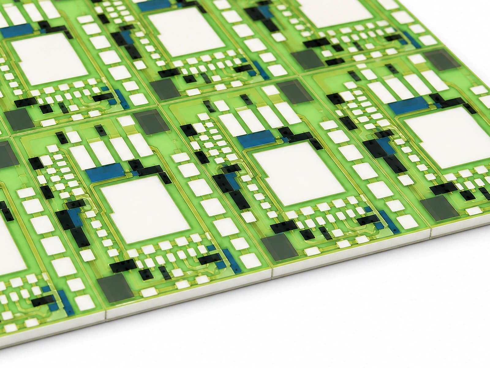
Review sensor inputsThe available views show an eight-position alumina panel with printed routes, white terminal areas, dark functional regions, blue features, green coverage, and visible ceramic edges. They support review of visible form only; they do not establish material purity, printed chemistry, dimensions, electrical results, lot identity, inspection records, or shipment traceability.
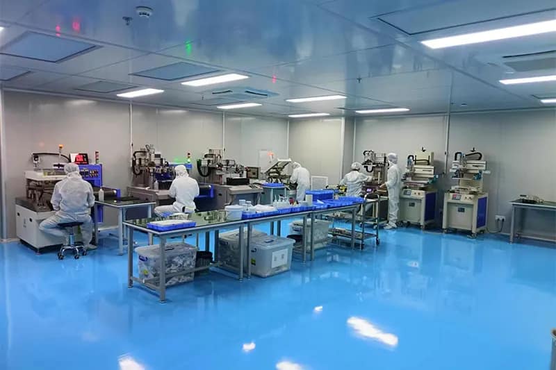
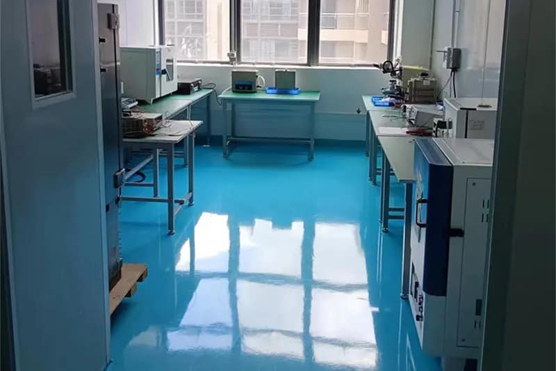
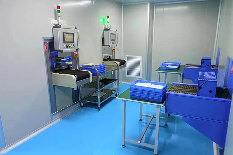
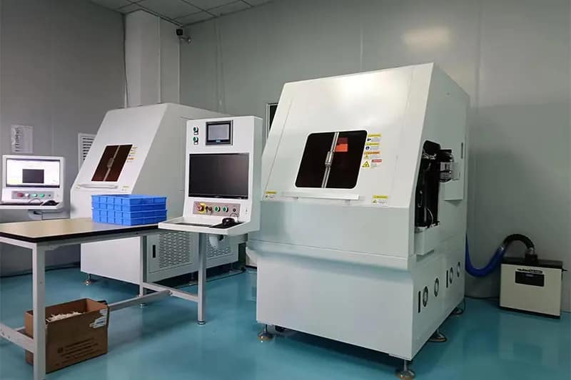
Company resources support thick film screen printing, controlled firing, route-dependent resistor trimming, and final inspection.
The applicable materials, artwork, thermal profile, trimming method, electrical checks, sampling, traceability, and acceptance records are confirmed for each released alumina circuit project.
Short answers for quotation planning; released drawings and validation requirements remain controlling.
Send the dimensioned drawing and artwork, alumina grade or required material data, thickness, conductor and functional-layer notes, electrical targets, assembly method, operating conditions, inspection criteria, quantity, schedule, and required records. PDF, Gerber, DXF, DWG, STEP, Excel, and clear sample photographs can support the first review.
They can be evaluated as a compatible project stack. The conductor, resistor, dielectric, protection, and terminal systems must match the selected alumina surface, print sequence, firing route, electrical duty, joining process, and validation method. A photograph or generic material name is not enough to release the construction.
The drawing should identify resistor geometry, target values, tolerance, TCR, power loading, test temperature, measurement points, and whether trimming is permitted. Engineering then reviews paste family, artwork allowance, firing interactions, trimming access, probe method, sampling, and the acceptance record required for the order.
Visual and dimensional checks form the usual starting point. Continuity, resistance, isolation, adhesion, solderability, wire-bond evaluation, thermal checks, traceability, and packing records can be added when the released drawing and purchase requirements define the method, sample size, limits, and document format.
Send enough information to connect the alumina substrate, printed stack, artwork, electrical function, assembly method, operating environment, inspection plan, and order scope. Clear sample photographs can begin a review when final CAD data is not ready.
PDF, DWG, DXF, STEP, Gerber, ZIP, Excel, Word, or sample photos are accepted.
The drawing-upload form loads as you reach this section.