Network material architecture
Select substrate, resistor paste families, conductor system, printed sequence, protection, and any multiple sheet-resistance ranges as a compatible fired construction.

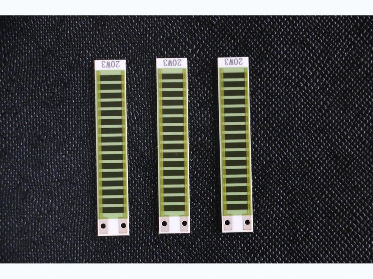
Multi-resistor custom ceramic network
Custom thick film resistor networks combine multiple drawing-defined resistors, conductor interconnects, and terminals on a compact ceramic substrate. Chipsimple reviews value range, ratios, tolerance, TCR tracking, loading, trim sequence, common nodes, terminal and package format, protection, heat distribution, environment, and test strategy as one network.
A drawing-controlled printed resistor network on a specified substrate, with circuit topology, terminals and any trimming operation defined for the intended electronics.
Send schematic and node names, target resistances and ratios, tolerances, temperature range, voltage and power per element, probe access, sample quantity and acceptance method.
Send DrawingsEvaluate settled code increments in a resistor-ladder conversion network using measured bit weights, explicit LSB conventions and major-carry error bounds.
Calculate the exact electrical output of a known bridge shunt, define its connection and gain-check boundary, and keep electrical verification separate from mechanical sensor calibration.
Separate common and differential resistor variation in a Wien-bridge network and calculate its zero-phase frequency and feedback attenuation with the actual capacitors.
Engineering method for independent network trim planning: compare electrically independent trim targets with coupled-target disturbance using bounded calculations, controlled evidence, failure signatures and drawing-specific release inputs.
Check whether temperature-dependent electrical power creates a growing common thermal mode when two coupled resistor channels operate together, despite stable single-channel tests.
Separate open leads, limited excitation and genuine high resistance using controlled fixture faults, instrument status and a valid measurement record.
Check a DAC output that calibrates correctly at DC but loses amplitude at higher signal frequency. Separate the hold response, resistor gain and reconstruction filter before changing the ceramic network.
Use a pairwise resistance fingerprint to verify terminal identity in a thick-film resistor network before ratio calibration can conceal a connection mistake.
Verified capability review
Custom Thick Film Resistor Network is shown against approved company capability control sheets.
Capability source: approved company category control sheets. Final values remain drawing- and sample-controlled.
| Parameter | Standard capability | Engineering review range | Final release |
|---|---|---|---|
| Substrate / Thickness | 96% / 99% Alumina / AlN; 0.25–3.0 mm | 96%/99% alumina or AlN within 0.25–3.0 mm, selected for thermal path, voltage, flatness, assembly, and firing | Approved material specification, drawing, and incoming criteria |
| Resistor System | RuO₂ / Cermet | RuO₂ or cermet selected for value, sheet resistance, TCR, load, stability, conductor, and firing compatibility | Released drawing and approved sample |
| Sheet Resistance | 1 Ω/□–1 MΩ/□ paste-family reference | Select within the 1 Ω/□–1 MΩ/□ paste-family reference after value, geometry, aspect ratio, and trim review | Released electrical limits, measurement method, and approved sample |
| Conductor System | Ag / Ag-Pd / Au | Ag, Ag-Pd, or Au selected for termination, bonding, soldering, voltage, environment, and firing | Approved material stack, assembly interface, and sample |
| Resistor Film Thickness | 8–15 µm fired typical | Within 8–15 µm fired typical, print build, firing, geometry, value distribution, and trimming are controlled | Released drawing, DFM approval, and first-article inspection |
| Firing Temperature | Up to 850°C | Peak up to 850°C; the actual profile, atmosphere, dwell, and refire sequence follow the selected paste system | Approved material-process route and production traveler |
| Parameter | Standard capability | Engineering review range | Final release |
|---|---|---|---|
| Resistance Value | 10 Ω–10 MΩ typical | Within 10 Ω–10 MΩ typical, nominal, ratio, reference temperature, voltage, and measurement method are defined | Released electrical limits, measurement method, and approved sample |
| Resistance Tolerance | ±1% standard | ±0.5% available after paste, geometry, trim allowance, TCR, stability, and measurement review | Released electrical limits, measurement method, and approved sample |
| TCR | ±100–200 ppm/°C typical | Within ±100–200 ppm/°C typical, define temperature interval, tracking, stabilization, and measurement method | Released electrical limits, measurement method, and approved sample |
| Laser Trimming | Passive / Active | Passive or active trimming with approved kerf, cut geometry, stopping rule, test condition, and post-trim protection | Released drawing and approved sample |
| Power / Working Voltage | By geometry and thermal design | Released from geometry, substrate, heat path, ambient, duty, pulse, clearance, field grading, and protection | Approved electrical-thermal design and instrumented prototype validation |
| Protection | Glass overglaze / Passivation | Glass overglaze or passivation selected for trim access, assembly, moisture, contamination, voltage, and temperature | Approved material stack, assembly interface, and sample |
Network engineering starts with the schematic and error budget. Review connects paste families, resistor geometry, common nodes, conductor resistance, ratio and TCR tracking, trim order, probe access, mutual heating, terminal parasitics, protection, mounting, environment, channel measurement, and any active adjustment condition.
Select substrate, resistor paste families, conductor system, printed sequence, protection, and any multiple sheet-resistance ranges as a compatible fired construction.
Release every resistor, common node, conductor, terminal, trim area, probe pad, spacing, identification, and package feature against the controlled schematic and value list.
Define absolute values, ratios, tolerance, TCR and tracking, voltage, power by element, mutual heating, lead or pad interface, mounting, and operating condition.
Specify passive or active trim order, channel measurement, probe points, stabilization, ratio calculation, isolation, visual checks, environment, sampling, and acceptance limits.
Custom networks reduce interconnect and footprint when the complete schematic, ratio error budget, loading, thermal coupling, package, and test route are controlled.
Application images are engineering illustrations, not customer projects, production records, or evidence of a released design. Suitability is confirmed only after the drawing, interfaces, operating conditions, risks, and validation plan are reviewed.
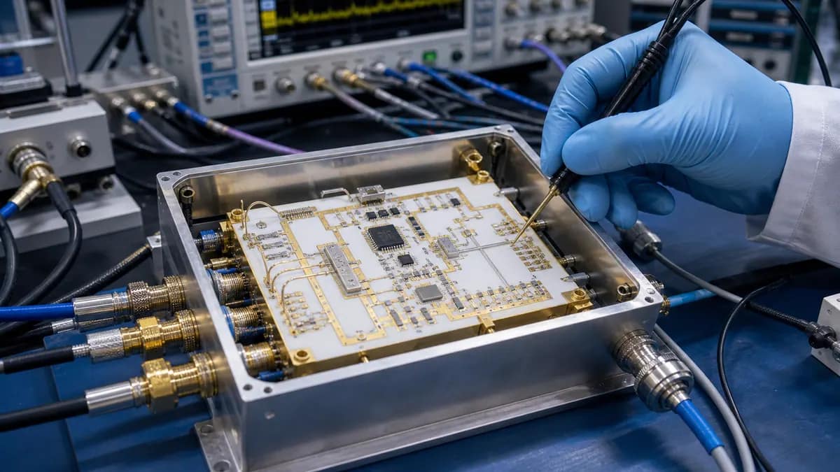 Application illustration
Compact matched networks require program-specific ratio, tracking, loading, bonding, protection, traceability, vibration, thermal cycling, and qualification.
Review application inputs Application illustration
Signal-conditioning networks need controlled ratios, drift, loading, cleanliness, assembly, calibration, documentation, and risk-based validation.
Review application inputs Application illustration
Networks can support sensing, biasing, attenuation, or termination after channel loading, isolation, heat, mounting, environment, and inspection are released.
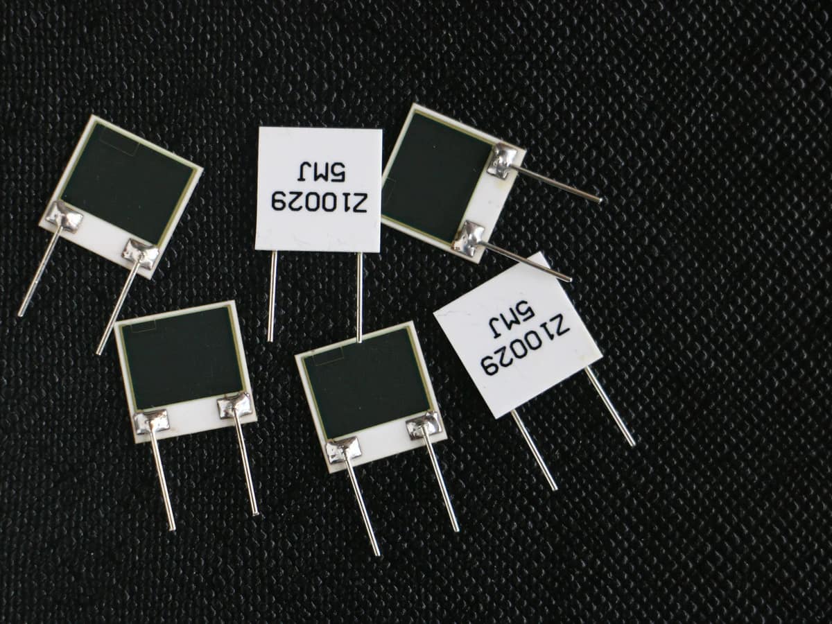
Review application inputsThe verified photographs show real thick film resistor networks in long, rectangular, square leaded, and round ceramic formats with printed resistor films, conductor terminals, and visible identification labels. They do not prove the marked value, internal schematic, ratios, tolerance, TCR, trim status, loading, or environmental qualification.
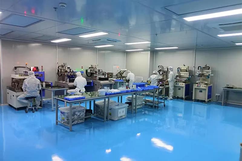
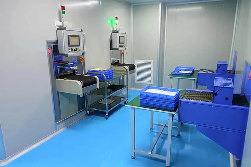
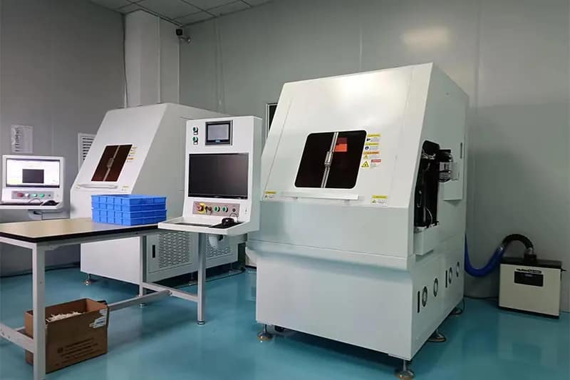
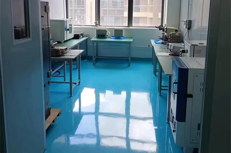
Chipsimple supports resistor printing, controlled firing, laser trimming, and laboratory inspection in Dongguan.
Network projects release the schematic, value and ratio table, artwork, trim order, channel test, loading, protection, sampling, traceability, and acceptance records together; matched performance requires the approved measurement conditions.
Short answers for quotation planning; released drawings and validation requirements remain controlling.
Provide the complete schematic, value and ratio table, tolerance, TCR and tracking requirements, common nodes, voltage and power by element, signal conditions, trim sequence, probe access, terminal or lead format, package dimensions, mounting, protection, environment, measurement order, and annual volume.
No. They are practical category-level selection values, not a released product specification. Material compatibility, geometry, print build, electrical loading, assembly, environment, inspection method, and expected volume can narrow the usable window. Final values are confirmed against the controlled drawing and approved project conditions.
Measure every channel and required ratio under controlled voltage, probe points, stabilization, sequence, and temperature. Include isolation, trim stability, TCR or tracking, loading and mutual-heating effects, terminal integrity, environmental stress, and long-term drift when required, with released sampling and failure limits.
Send the controlled drawing or artwork, dimensions and tolerances, material preference, electrical targets, assembly interface, operating environment, validation requirements, prototype quantity, annual volume, and schedule. Include the schematic, value and ratio table, per-element loading, TCR tracking, trim order, terminals, package, and channel test sequence.
Send the schematic and complete value, ratio, TCR, loading, terminal, package, trim, and test definitions. A useful network quotation depends on how channels interact and are measured; a list of nominal values without topology and operating conditions is not enough for release.
PDF, DWG, DXF, STEP, Gerber, ZIP, Excel, Word, or sample photos are accepted.
The drawing-upload form loads as you reach this section.