Ceramic and resistor system
Confirm substrate grade and thickness, resistor paste, conductor and terminal route, film build, firing, trim allowance, protection, edge finish, and material compatibility.

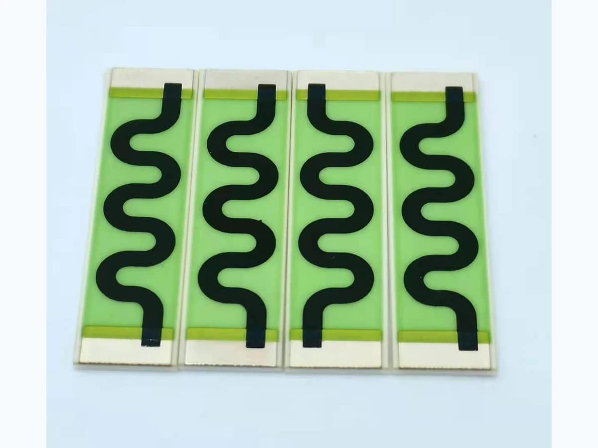
Custom high-voltage resistive element
High voltage thick film resistors use long, drawing-controlled resistive paths on ceramic to distribute voltage while meeting resistance, power, and package constraints. Chipsimple reviews working and overload voltage, value, tolerance, TCR, geometry, voltage gradient, creepage, terminals, protection, pulse duty, mounting, contamination, and validation together.
Verified capability review
High Voltage Thick Film Resistor is shown against approved company capability control sheets.
Capability source: approved company category control sheets. Final values remain drawing- and sample-controlled.
| Parameter | Standard capability | Engineering review range | Final release |
|---|---|---|---|
| Substrate / Thickness | 96% / 99% Alumina / AlN; 0.25–3.0 mm | 96%/99% alumina or AlN within 0.25–3.0 mm, selected for thermal path, voltage, flatness, assembly, and firing | Approved material specification, drawing, and incoming criteria |
| Resistor System | RuO₂ / Cermet | RuO₂ or cermet selected for value, sheet resistance, TCR, load, stability, conductor, and firing compatibility | Released drawing and approved sample |
| Sheet Resistance | 1 Ω/□–1 MΩ/□ paste-family reference | Select within the 1 Ω/□–1 MΩ/□ paste-family reference after value, geometry, aspect ratio, and trim review | Released electrical limits, measurement method, and approved sample |
| Conductor System | Ag / Ag-Pd / Au | Ag, Ag-Pd, or Au selected for termination, bonding, soldering, voltage, environment, and firing | Approved material stack, assembly interface, and sample |
| Resistor Film Thickness | 8–15 µm fired typical | Within 8–15 µm fired typical, print build, firing, geometry, value distribution, and trimming are controlled | Released drawing, DFM approval, and first-article inspection |
| Firing Temperature | Up to 850°C | Peak up to 850°C; the actual profile, atmosphere, dwell, and refire sequence follow the selected paste system | Approved material-process route and production traveler |
| Parameter | Standard capability | Engineering review range | Final release |
|---|---|---|---|
| Resistance Value | 10 Ω–10 MΩ typical | Within 10 Ω–10 MΩ typical, nominal, ratio, reference temperature, voltage, and measurement method are defined | Released electrical limits, measurement method, and approved sample |
| Resistance Tolerance | ±1% standard | ±0.5% available after paste, geometry, trim allowance, TCR, stability, and measurement review | Released electrical limits, measurement method, and approved sample |
| TCR | ±100–200 ppm/°C typical | Within ±100–200 ppm/°C typical, define temperature interval, tracking, stabilization, and measurement method | Released electrical limits, measurement method, and approved sample |
| Laser Trimming | Passive / Active | Passive or active trimming with approved kerf, cut geometry, stopping rule, test condition, and post-trim protection | Released drawing and approved sample |
| Power / Working Voltage | By geometry and thermal design | Released from geometry, substrate, heat path, ambient, duty, pulse, clearance, field grading, and protection | Approved electrical-thermal design and instrumented prototype validation |
| Protection | Glass overglaze / Passivation | Glass overglaze or passivation selected for trim access, assembly, moisture, contamination, voltage, and temperature | Approved material stack, assembly interface, and sample |
High-voltage review begins with the voltage waveform and insulation environment. Engineering connects resistor sheet family and path, local voltage gradient, conductor overlap, trim geometry, creepage and clearance, edge condition, protective coating, terminal field concentration, power and pulse heating, mounting, humidity, contamination, altitude, and safe test fixtures.
Confirm substrate grade and thickness, resistor paste, conductor and terminal route, film build, firing, trim allowance, protection, edge finish, and material compatibility.
Release path width and spacing, turns, overlaps, trim area, terminal separation, edge distance, creepage route, coating windows, and dimensional tolerances.
Separate continuous working voltage, overload, surge or pulse waveform, energy, repetition, resistance, current, power, ambient, altitude, mounting, and cooling.
Specify resistance, visual and dimensional checks, working and overload tests, leakage or isolation, pulse verification, temperature rise, humidity, coating, fixture safety, sampling, and limits.
High-voltage resistors fit dividers, bleeders, sensing, and discharge functions only after waveform, insulation environment, mounting, protection, and fault conditions are defined.
Application images are engineering illustrations, not customer projects, production records, or evidence of a released design. Suitability is confirmed only after the drawing, interfaces, operating conditions, risks, and validation plan are reviewed.
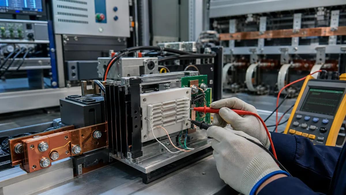 Application illustration
Power systems require released working and surge voltage, discharge energy, isolation, mounting, pollution, altitude, thermal path, fault behavior, and safety tests.
Review application inputs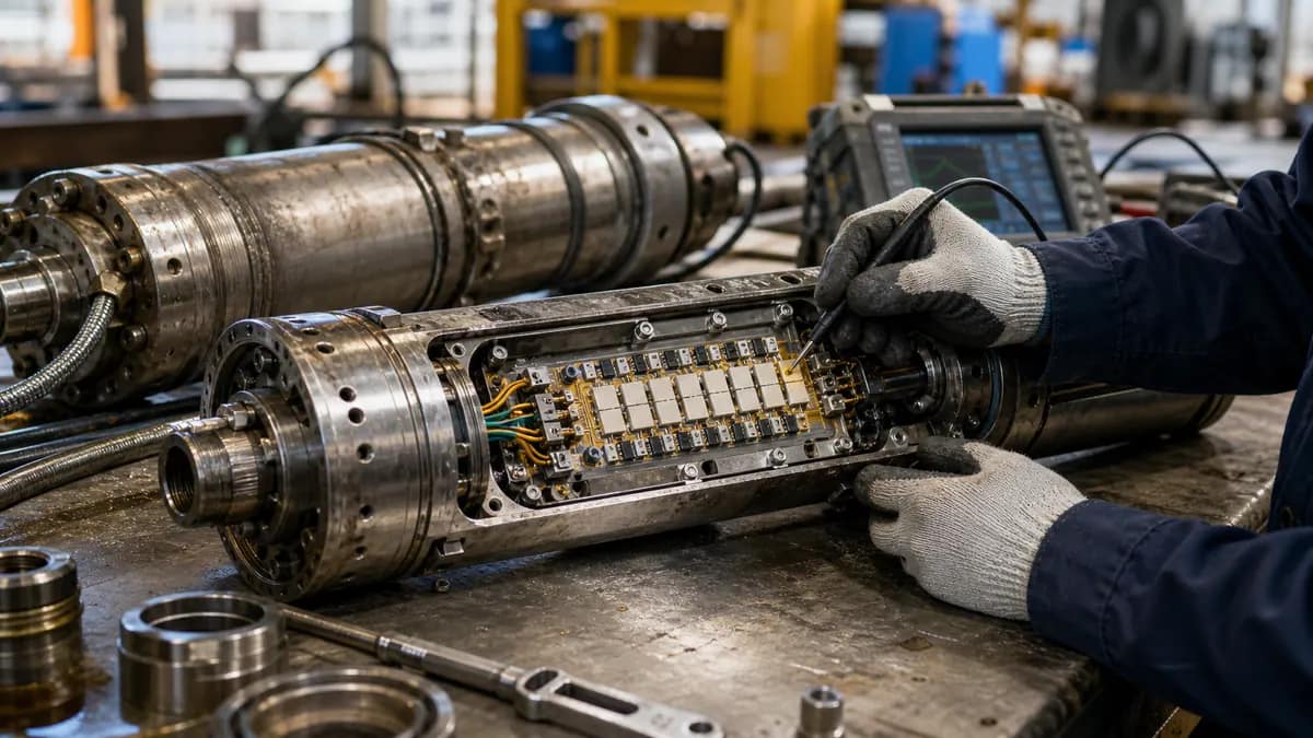 Application illustration
Instrumentation in demanding environments needs application-specific voltage, temperature, contamination, pressure or media isolation, coating, terminals, and reliability validation.
Review application inputs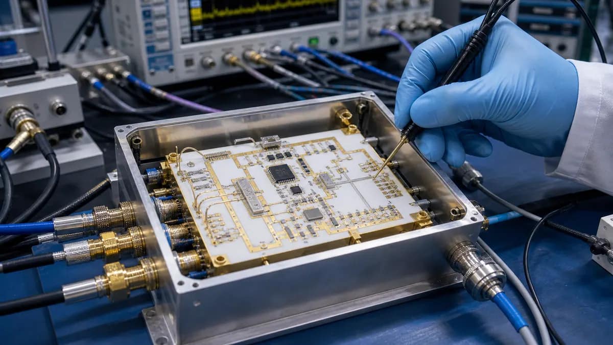 Application illustration
Aviation and industrial programs require controlled derating, altitude, transient waveforms, vibration, thermal cycling, traceability, protection, and qualification evidence.
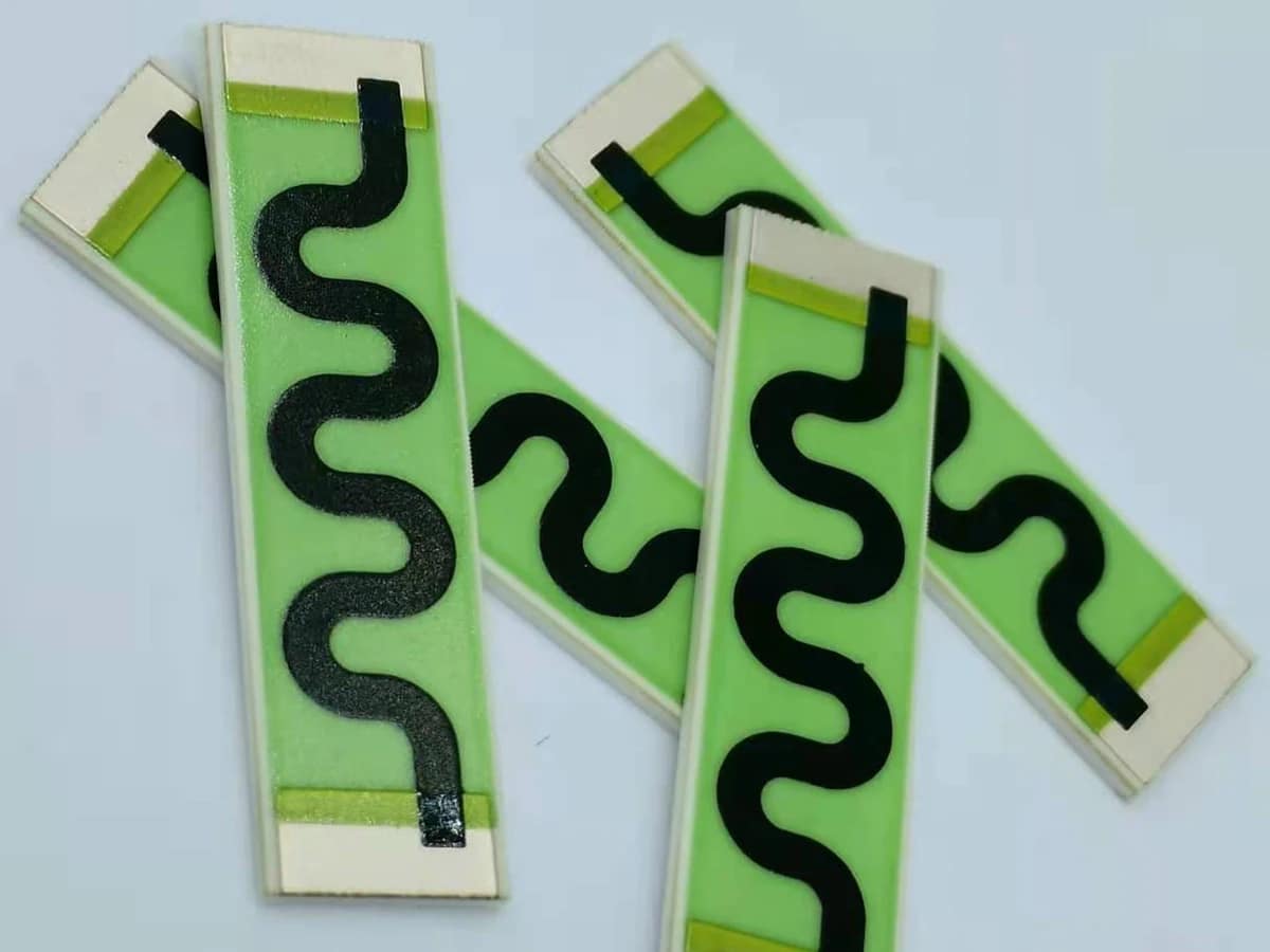
Review application inputsFive selected verified photographs show real long ceramic resistor strips with black serpentine paths, green areas, conductor overlaps, and end terminals. Surface geometry does not prove resistance, TCR, working voltage, overload, pulse energy, creepage performance, coating chemistry, power, or environmental reliability.
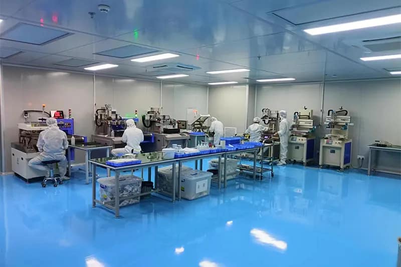
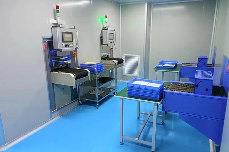
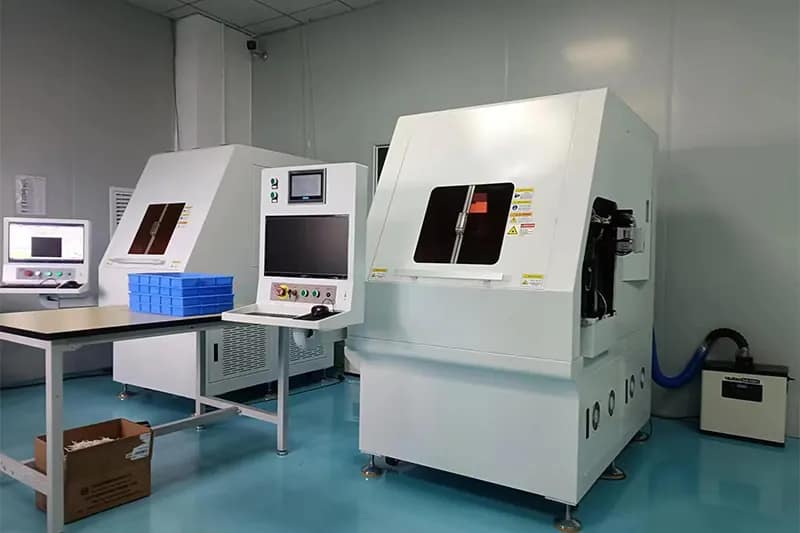
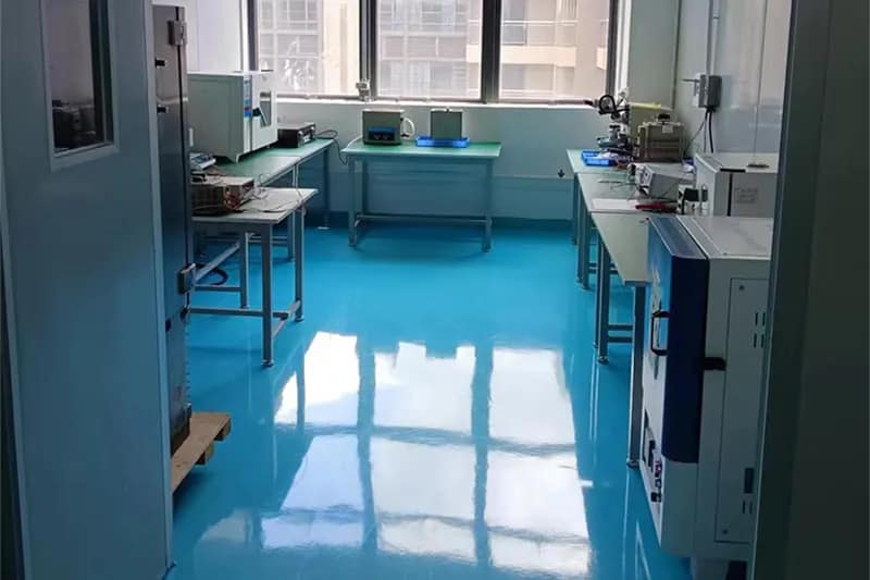
Chipsimple supports resistor printing, controlled firing, laser trimming, and laboratory inspection in Dongguan.
High-voltage projects release the material stack, artwork, trim instruction, voltage and pulse fixtures, protection, loading, sampling, traceability, and acceptance records together; final ratings require project-specific electrical and environmental validation.
Short answers for quotation planning; released drawings and validation requirements remain controlling.
Define resistance, tolerance, TCR, continuous working voltage, overload, surge or pulse waveform and energy, repetition, power, current, ambient, altitude, pollution or contamination, creepage and clearance, protection, terminals, mounting, cooling, fault conditions, derating, and required safety or reliability tests.
No. They are practical category-level selection values, not a released product specification. Material compatibility, geometry, print build, electrical loading, assembly, environment, inspection method, and expected volume can narrow the usable window. Final values are confirmed against the controlled drawing and approved project conditions.
Verify resistance and dimensions, then continuous voltage, overload or pulse behavior, leakage or isolation as applicable, temperature rise, coating and terminal condition, humidity, contamination, altitude or pressure effects, and cycling using guarded fixtures, controlled waveforms, derating, sampling, and failure limits.
Send the controlled drawing or artwork, dimensions and tolerances, material preference, electrical targets, assembly interface, operating environment, validation requirements, prototype quantity, annual volume, and schedule. Include working and overload voltage, pulse waveform and energy, repetition, derating, creepage environment, altitude, protection, mounting, and safe test limits.
Send the complete voltage waveform and insulation environment with the resistor drawing. Working voltage, overload, pulse energy, path geometry, creepage, protection, terminals, power, mounting, altitude, contamination, and test safety determine the route; resistance value alone cannot release a high-voltage design.
PDF, DWG, DXF, STEP, Gerber, ZIP, Excel, Word, or sample photos are accepted.
The drawing-upload form loads as you reach this section.