Resistive and collector system
Select the carbon system, conductor interface, film build, cure, protection, exposed contact windows, and collector arrangement as one compatible printed stack.

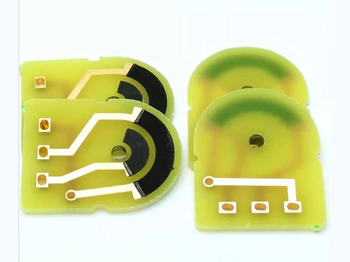
Custom printed potentiometer element
Carbon film potentiometer PCBs integrate a printed resistive track and conductor interface on FR-4 for rotary or application-specific adjustment. Chipsimple reviews resistance range, taper or curve, active angle, wiper geometry and force, copper overlap, terminals, loading, protection, wear duty, environment, and calibration together.
Verified capability review
Carbon Film Potentiometer PCB is shown against approved company capability control sheets.
Capability source: approved company category control sheets. Final values remain drawing- and sample-controlled.
| Parameter | Standard capability | Engineering review range | Final release |
|---|---|---|---|
| Base Material | FR-4 | FR-4 grade, Tg, copper construction, finish, mask, and panel route by PCB and cure review | Approved material specification, drawing, and incoming criteria |
| Board Thickness | 0.4–3.2 mm typical | Within 0.4–3.2 mm typical, stack, tolerance, flatness, connector, and enclosure are reviewed | Approved material specification, drawing, and incoming criteria |
| Copper Weight | 0.5–2 oz typical | Within 0.5–2 oz typical, current, pad geometry, carbon overlap, etch, and finish are reviewed | Released drawing and approved sample |
| Carbon Ink | Polymer carbon / Ag-C blend | Polymer carbon or Ag-C blend selected for resistor, contact, curve, or jumper function | Released drawing and approved sample |
| Carbon Film Thickness | 8–15 µm typical | Within 8–15 µm typical, screen, cure, sheet resistance, adhesion, and wear are controlled together | Released drawing, DFM approval, and first-article inspection |
| Cure Temperature | 120–150°C typical | Within 120–150°C typical, peak, dwell, support, board finish, and warpage are validated | Approved material-process route and production traveler |
| Parameter | Standard capability | Engineering review range | Final release |
|---|---|---|---|
| Sheet Resistance | 50–5,000 Ω/□/25 µm reference | Select within the 50–5,000 Ω/□/25 µm ink-family reference after geometry and target review | Released electrical limits, measurement method, and approved sample |
| Target Resistance | 10 Ω–1 MΩ typical | Within 10 Ω–1 MΩ typical, measurement points, temperature, loading, geometry, and tolerance are defined | Released electrical limits, measurement method, and approved sample |
| Resistance Tolerance | ±5% / ±10% typical | ±5% or ±10% selected by ink, geometry, copper overlap, cure, and measurement method | Released electrical limits, measurement method, and approved sample |
| Linearity | ±1–5% FS typical | Within ±1–5% FS typical, define calculation method, active travel, endpoints, hysteresis, and loading | Released electrical limits, measurement method, and approved sample |
| Surface Finish | HASL / ENIG / ENEPIG | HASL, ENIG, or ENEPIG selected for carbon compatibility, soldering, contact, corrosion, and storage | Approved material stack, assembly interface, and sample |
| Wear Life | ≥10,000 cycles typical | Beyond the ≥10,000-cycle typical basis, define mating contact, force, speed, stroke, current, lubricant, and drift limit | Agreed lifecycle profile, acceptance drift, and validation report |
Potentiometer performance is set by the entire electromechanical chain. Engineering review connects track aspect ratio and sheet resistance, conductor overlap, collector path, active angle, taper table, wiper material and force, shaft alignment, electrical loading, protection, contamination, movement duty, and calibration method.
Select the carbon system, conductor interface, film build, cure, protection, exposed contact windows, and collector arrangement as one compatible printed stack.
Release active and total angle, start and end references, track width, collector geometry, overlaps, dead zones, terminals, and the required resistance or voltage curve.
Define wiper material, number of fingers, force, radius, alignment, rotation direction, speed, stops, lubrication, housing support, and assembly tolerances.
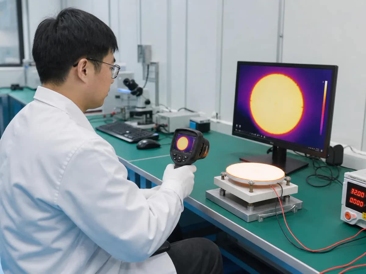
Specify measurement points, electrical loading, linearity or taper error, contact resistance variation, repeatability, rotation cycles, environment, and calibrated fixture limits.
Printed potentiometer boards support rotary feedback and manual adjustment only after the wiper, shaft, electronics, enclosure, and validation conditions are defined.
Application images are engineering illustrations, not customer projects, production records, or evidence of a released design. Suitability is confirmed only after the drawing, interfaces, operating conditions, risks, and validation plan are reviewed.
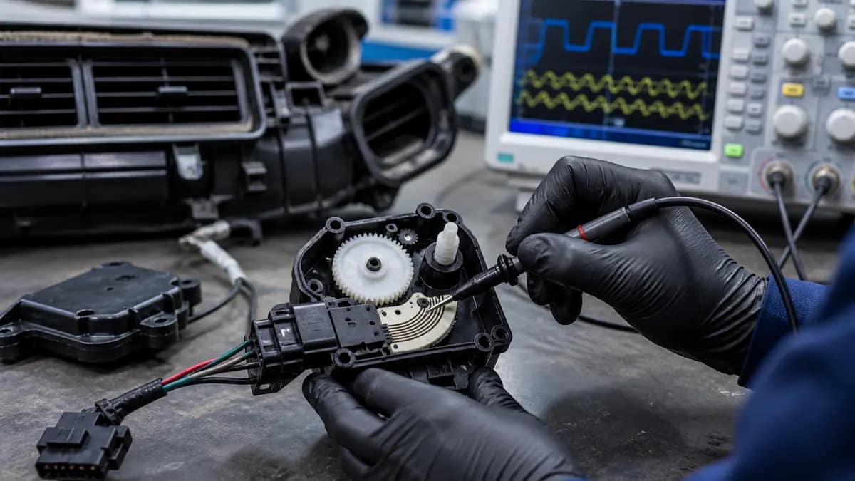 Application illustration
Arc tracks can be evaluated for actuator position feedback when gear travel, wiper force, connector, temperature, vibration, calibration, and expected cycles are released.
Review application inputs Application illustration
Compact rotary feedback requires application-specific resolution, taper, speed, support, contact behavior, control electronics, duty cycle, and environmental validation.
Review application inputs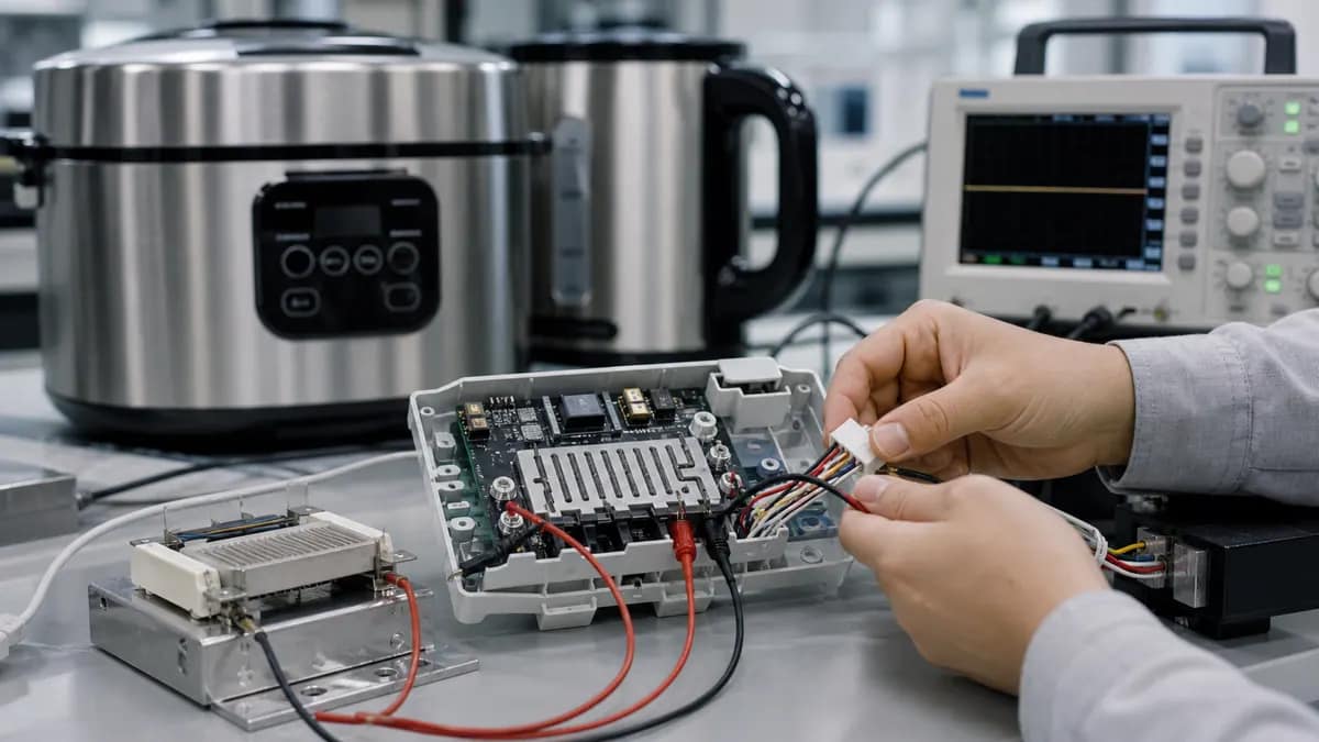 Application illustration
Control knobs and selector assemblies may use printed tracks after detents, shaft alignment, current, cleaning, humidity, feel, and lifecycle targets are defined.
Review application inputsThe verified product views show arc-shaped black printed tracks, circular openings, conductor and terminal regions, and several board arrangements. They do not establish resistance value, taper, active angle, linearity, contact noise, wiper compatibility, torque, wear life, or environmental performance.
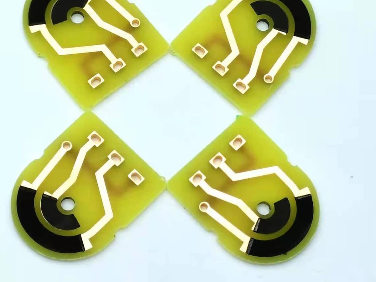
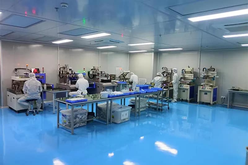
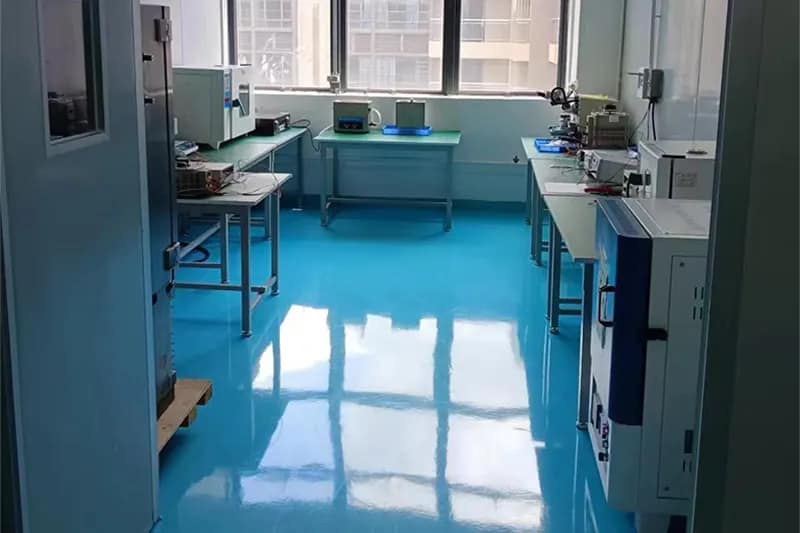
Chipsimple supports polymer-carbon printing, laboratory inspection, managed production, and protected packing in Dongguan.
Potentiometer projects release the board and ink system, track artwork, wiper fixture, curve test, sampling, traceability, and acceptance criteria together; completed-control performance remains tied to the customer mechanism.
Short answers for quotation planning; released drawings and validation requirements remain controlling.
Define resistance range, taper or curve table, total and active angle, direction, terminal references, electrical loading, wiper material and force, shaft and housing alignment, rotational speed, expected cycles, contamination, temperature, humidity, connector, calibration, and acceptance method before artwork release.
No. They are practical category-level selection values, not a released product specification. Material compatibility, geometry, print build, electrical loading, assembly, environment, inspection method, and expected volume can narrow the usable window. Final values are confirmed against the controlled drawing and approved project conditions.
Use the production-intent wiper, shaft support, and electronics to measure resistance or voltage against angle, taper error, repeatability, contact noise, end behavior, temperature effects, contamination, and wear. The fixture, speed, force, current, conditioning, sample size, and failure limits must be controlled.
Send the controlled drawing or artwork, dimensions and tolerances, material preference, electrical targets, assembly interface, operating environment, validation requirements, prototype quantity, annual volume, and schedule. Include the taper or curve table, angle references, wiper design and force, shaft alignment, electrical load, and target cycles.
Provide the board artwork and the complete rotary interface so track geometry, taper, wiper mechanics, electrical loading, protection, calibration, and wear validation can be reviewed as one product. A curve table and controlled angle references are more useful than a nominal resistance alone.
PDF, DWG, DXF, STEP, Gerber, ZIP, Excel, Word, or sample photos are accepted.
The drawing-upload form loads as you reach this section.