Jumper material and stack
Confirm FR-4 and copper construction, carbon system, printed film build, cure, any insulating layer beneath the jumper, and protection above exposed or non-contact areas.

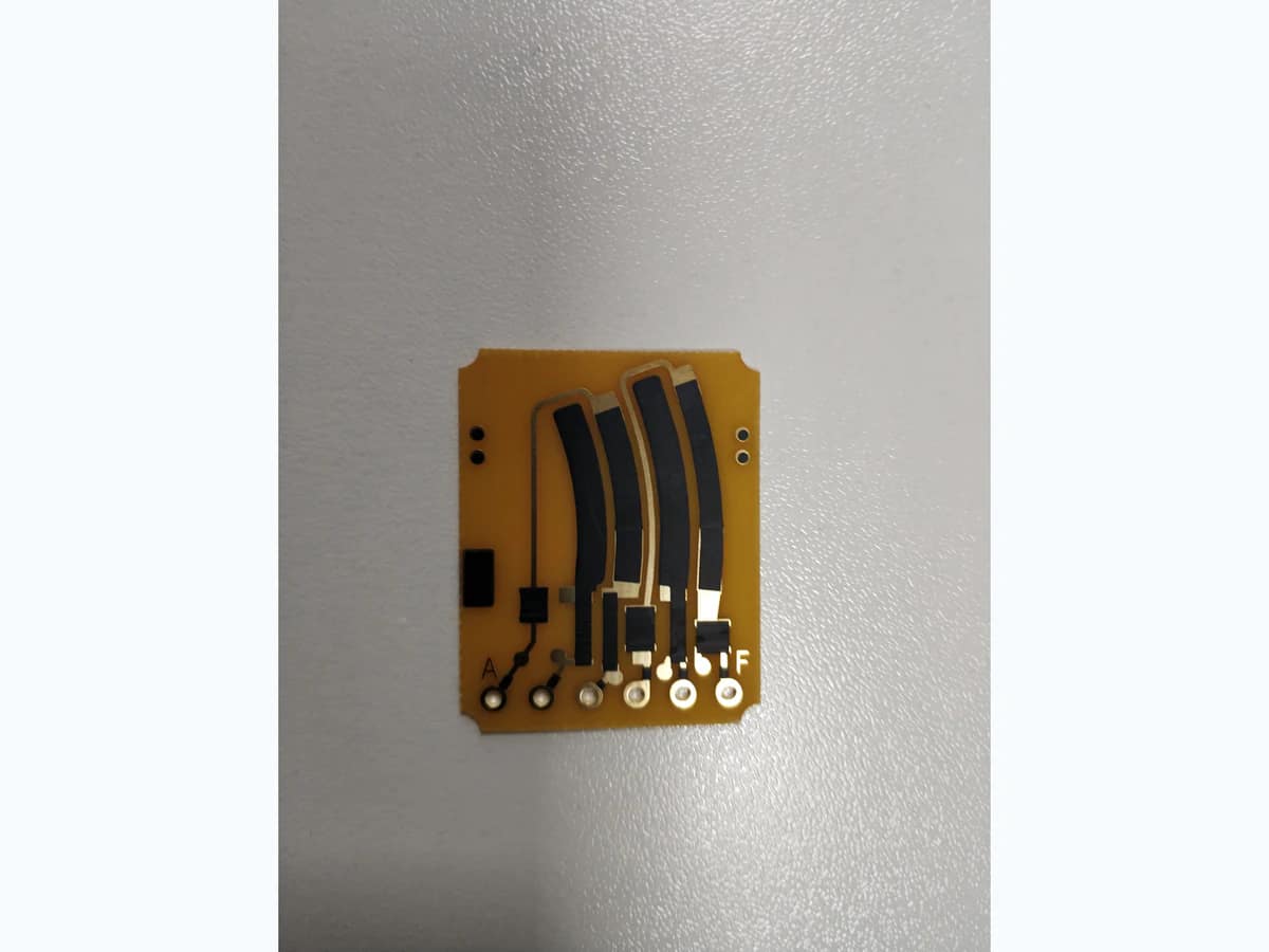
Printed carbon crossover circuit
Carbon ink jumper PCBs use a printed carbon path to connect drawing-selected nodes on an FR-4 circuit where the artwork and electrical duty suit the material system. Chipsimple reviews jumper geometry, copper overlap, underlying insulation, resistance, current, voltage, cure, protection, spacing, and test limits before release.
Verified capability review
Carbon Ink Jumper PCB is shown against approved company capability control sheets.
Capability source: approved company category control sheets. Final values remain drawing- and sample-controlled.
| Parameter | Standard capability | Engineering review range | Final release |
|---|---|---|---|
| Base Material | FR-4 | FR-4 grade, Tg, copper construction, finish, mask, and panel route by PCB and cure review | Approved material specification, drawing, and incoming criteria |
| Board Thickness | 0.4–3.2 mm typical | Within 0.4–3.2 mm typical, stack, tolerance, flatness, connector, and enclosure are reviewed | Approved material specification, drawing, and incoming criteria |
| Copper Weight | 0.5–2 oz typical | Within 0.5–2 oz typical, current, pad geometry, carbon overlap, etch, and finish are reviewed | Released drawing and approved sample |
| Carbon Ink | Polymer carbon / Ag-C blend | Polymer carbon or Ag-C blend selected for resistor, contact, curve, or jumper function | Released drawing and approved sample |
| Carbon Film Thickness | 8–15 µm typical | Within 8–15 µm typical, screen, cure, sheet resistance, adhesion, and wear are controlled together | Released drawing, DFM approval, and first-article inspection |
| Cure Temperature | 120–150°C typical | Within 120–150°C typical, peak, dwell, support, board finish, and warpage are validated | Approved material-process route and production traveler |
| Parameter | Standard capability | Engineering review range | Final release |
|---|---|---|---|
| Sheet Resistance | 50–5,000 Ω/□/25 µm reference | Select within the 50–5,000 Ω/□/25 µm ink-family reference after geometry and target review | Released electrical limits, measurement method, and approved sample |
| Target Resistance | 10 Ω–1 MΩ typical | Within 10 Ω–1 MΩ typical, measurement points, temperature, loading, geometry, and tolerance are defined | Released electrical limits, measurement method, and approved sample |
| Resistance Tolerance | ±5% / ±10% typical | ±5% or ±10% selected by ink, geometry, copper overlap, cure, and measurement method | Released electrical limits, measurement method, and approved sample |
| Linearity | ±1–5% FS typical | Within ±1–5% FS typical, define calculation method, active travel, endpoints, hysteresis, and loading | Released electrical limits, measurement method, and approved sample |
| Surface Finish | HASL / ENIG / ENEPIG | HASL, ENIG, or ENEPIG selected for carbon compatibility, soldering, contact, corrosion, and storage | Approved material stack, assembly interface, and sample |
| Wear Life | ≥10,000 cycles typical | Beyond the ≥10,000-cycle typical basis, define mating contact, force, speed, stroke, current, lubricant, and drift limit | Agreed lifecycle profile, acceptance drift, and validation report |
A reliable printed jumper depends on the complete current path and isolation structure. Engineering review connects carbon sheet resistance, path aspect ratio, copper overlap, surface finish, underlying mask or dielectric, adjacent-node voltage, current and duty, heat rise, contamination, cure, protection, and the electrical test method.
Confirm FR-4 and copper construction, carbon system, printed film build, cure, any insulating layer beneath the jumper, and protection above exposed or non-contact areas.
Release jumper width and length, copper landing overlap, crossings, keep-outs, adjacent-node spacing, mask openings, and registration tolerances in controlled artwork.
Define target resistance or maximum drop, current, voltage, duty cycle, ambient temperature, allowable heat rise, fault condition, and any downstream soldering or cleaning exposure.
Specify resistance, continuity, open/short, adjacent-net isolation, visual coverage, adhesion, environment, sampling, fixture, current, and acceptance limits for release.
Printed jumpers can simplify selected low-current routing when the board stack, isolation, voltage, thermal behavior, and electrical test are compatible with the application.
Application images are engineering illustrations, not customer projects, production records, or evidence of a released design. Suitability is confirmed only after the drawing, interfaces, operating conditions, risks, and validation plan are reviewed.
 Application illustration
Printed jumpers may support constrained routing after node voltage, current, isolation, enclosure contamination, assembly heat, and field-duty requirements are reviewed.
Review application inputs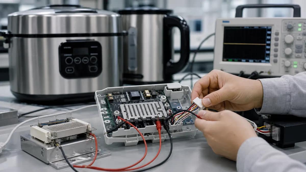 Application illustration
Low-current appliance controls can be evaluated when moisture, cleaning, mains separation, temperature, soldering, fault behavior, and safety requirements are defined.
Review application inputs Application illustration
Compact instrument circuits require controlled voltage, leakage, cleaning, material declaration, inspection, and risk-based validation before a printed jumper route is approved.
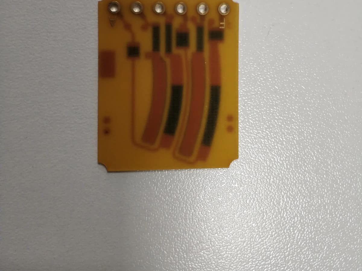
Review application inputsFour unique supplied photographs and one controlled detail crop show real FR-4 boards with black printed jumper paths, conductor interfaces, pads, holes, and several geometries. They do not prove net assignment, insulation beneath a crossing, resistance, current rating, voltage isolation, adhesion, or lifecycle performance.
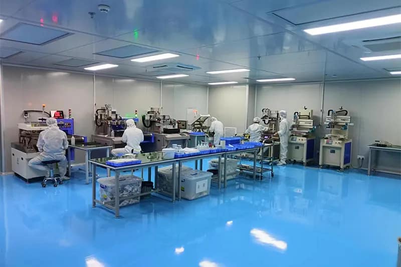
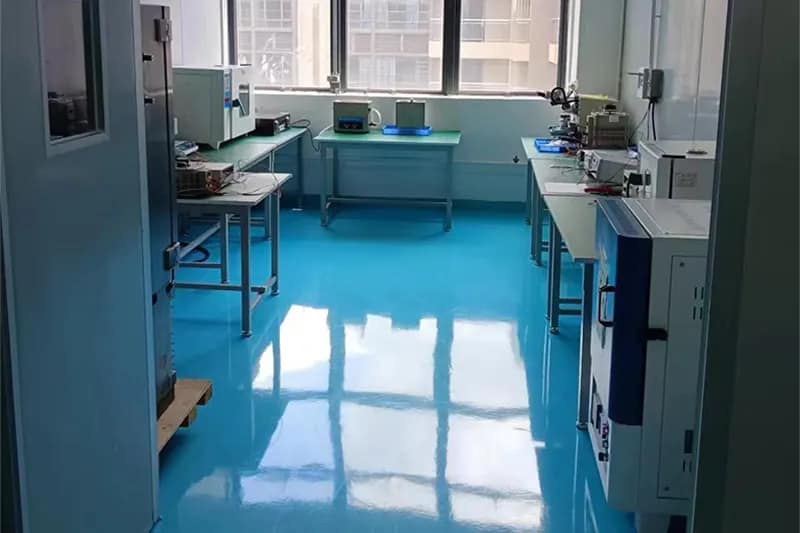
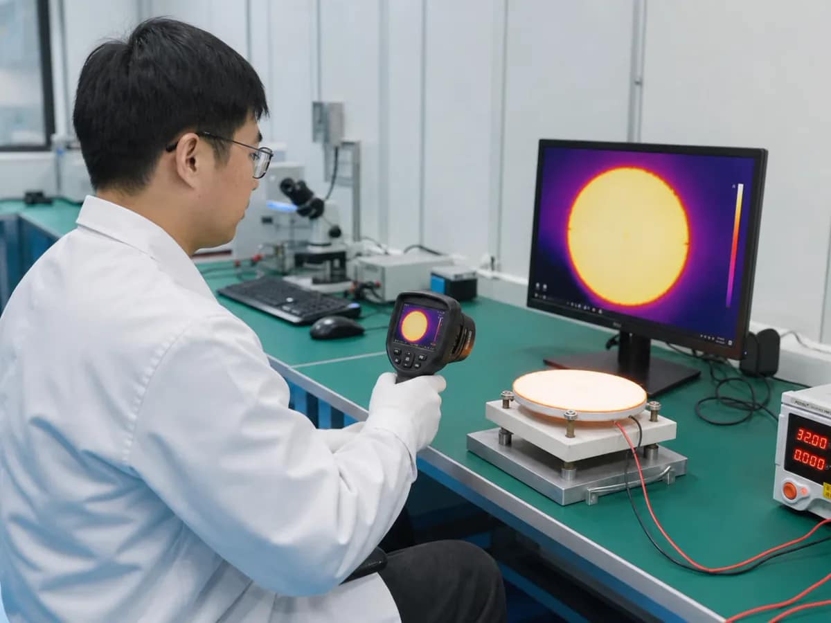
Chipsimple supports polymer-carbon printing, laboratory inspection, managed production, and protected packing in Dongguan.
Jumper projects release the board stack, artwork, carbon and insulating systems, cure route, electrical test, sampling, traceability, and acceptance criteria together; current and isolation capability remain project-specific.
Short answers for quotation planning; released drawings and validation requirements remain controlling.
Define the connected nets, path and crossing artwork, board stack, copper finish, underlying insulation, carbon system, target or maximum resistance, current, voltage, duty cycle, spacing, allowable heat rise, protection, soldering and cleaning exposure, environment, and electrical test limits before selecting this route.
No. They are practical category-level selection values, not a released product specification. Material compatibility, geometry, print build, electrical loading, assembly, environment, inspection method, and expected volume can narrow the usable window. Final values are confirmed against the controlled drawing and approved project conditions.
Verify visual coverage and registration, jumper resistance and continuity, open/short behavior, adjacent-net isolation, voltage drop or heat rise at the released load, adhesion, assembly exposure, and project-selected temperature or humidity tests. Use controlled fixtures, conditioning, sample sizes, and failure limits.
Send the controlled drawing or artwork, dimensions and tolerances, material preference, electrical targets, assembly interface, operating environment, validation requirements, prototype quantity, annual volume, and schedule. Identify every connected net and crossing, the insulating structure, maximum resistance, current, voltage, duty, and isolation test.
Send the board data with net assignments and electrical duty so the jumper path, copper overlap, isolation stack, current, resistance, voltage, protection, cure, and test route can be assessed. A printed crossover should be approved from circuit risk, not selected from appearance alone.
PDF, DWG, DXF, STEP, Gerber, ZIP, Excel, Word, or sample photos are accepted.
The drawing-upload form loads as you reach this section.