
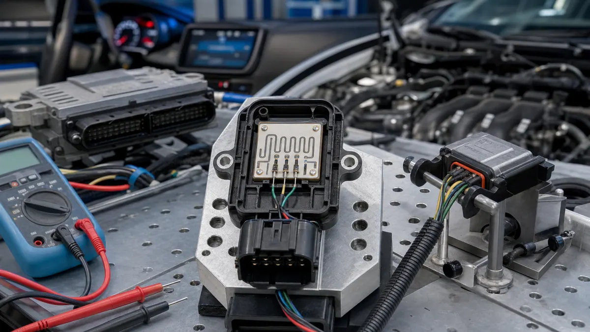
Thick film circuit quality depends on the ceramic substrate before any paste is printed. Material grade, forming method, sintering shrinkage, flatness, surface finish, machining, and inspection can all affect conductor adhesion, resistor stability, dielectric integrity, and assembly fit.
Material selection
Alumina is widely used for cost-effective thick film ceramic circuits. Aluminum nitride is selected when thermal conductivity is more important. Other advanced ceramics may be useful for structural, chemical, or high-temperature requirements, but paste compatibility and cost must be reviewed.
Forming and sintering considerations
Ceramic parts shrink during firing. Substrate manufacturers compensate for this shrinkage through tooling and process control. For thick film circuits, dimensional stability, flatness, and surface condition are important because printed layers must register correctly and fire consistently.
Machining and features
- Holes, slots, chamfers, and edge profiles should be defined before print design is finalized.
- Sharp inside corners can create handling risk and stress concentration.
- Surface roughness affects paste wetting and adhesion.
- Very tight ceramic tolerances may require additional grinding or laser machining.
Inspection before printing
Substrate inspection should check size, thickness, flatness, cracks, chips, warpage, surface contamination, and hole quality. Defects that look minor before printing can become serious after firing or assembly.
RFQ data for ceramic thick film substrates
Provide material grade, thickness, outline, tolerance, hole pattern, surface finish, flatness, expected firing process, printed layer stack, and operating environment. If the substrate is part of a sensor, heater, or power module, include the full application requirement rather than only ceramic dimensions.