Incoming and mechanical
Material identity, drawing revision, outline, thickness, holes, slots, surface condition, flatness or bow where specified, and handling damage.

Chipsimple reviews custom ceramic circuits, printed resistors, sensor elements, heaters, hybrid substrates, and selected polymer or FR-4 printed functions from RFQ through prototype and repeat-production release.
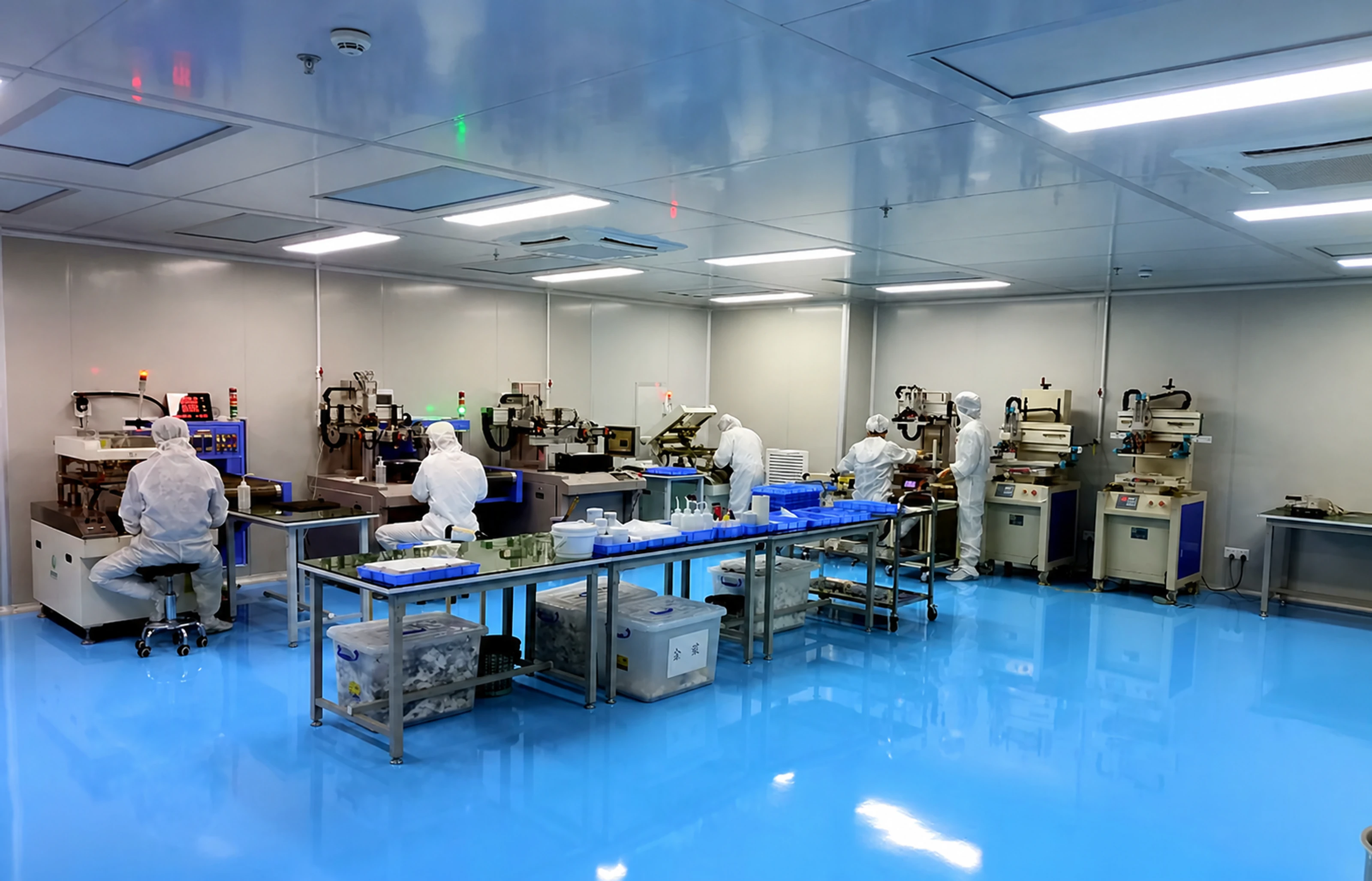
The factory confirms support for the capability ranges published below. They define our available manufacturing envelope, while the released part specification remains controlled by the selected substrate and material system, geometry, assembly, test method, order volume, and approved drawing.
Seven engineering tables bring substrate, ceramic process, printed resistor, conductor, resistive, dielectric, and insulating material capabilities into one reviewable manufacturing reference.
Confirmed ceramic substrate families and the material/application envelope available for engineering selection.
| Property | Alumina (Al₂O₃) | Aluminum Nitride (AlN) | Beryllium Oxide (BeO) | Zirconium Dioxide (ZrO₂) |
|---|---|---|---|---|
| Maximum application temperature (°F) | 662–1,832 | 1,832 | 2,300 | 2,432 |
| Maximum power density (W/in²) | 75 | 1,010 | 250 | 300 |
| Maximum ramp-up speed (°F/s) | 122 | 572 | 400 | 350 |
| Thermal conductivity (W/m·K) | 20–35 | 180–220 | 200–300 | 2.0–5.0 |
| Density (g/cm³) | 3.75 | 3.26 | 2.8 | 5.9 |
| Dielectric loss | 0.0001–0.001 | 0.0001–0.0005 | 0.0001–0.0002 | 0.0005–0.001 |
| Dielectric constant | 9.4–10.2 | 8.5–9.0 | 6.0–7.0 | 25–30 |
| CTE (ppm/°C) | 6.0–8.0 | 4.0–5.0 | 7.0–9.0 | 10.0–11.0 |
| Substrate thickness (mm) | 0.25–2.0 | 0.25–2.0 | 0.25–2.0 | 0.25–2.0 |
| Typical maximum dimension (in) | 6 × 12 | 5 × 11 | 6 × 6 | 4 × 4 |
| Theoretical total wattage (W) | 5,400 | 55,000 | 15,000 | 20,000 |
Release note: Material properties and thermal limits are matched to the selected grade and supplier data. Final part performance also depends on geometry, metallization, assembly, heat path, and validation method.
Covered metallization families include screen-printed thick-film substrates and photo-imaged thin-film substrates. The matrix also records adjacent ceramic process routes available for project review.
| Process parameter | TFM | HTCC / LTCC | DBC | DPC | AMB |
|---|---|---|---|---|---|
| Layer counts | 1, 2, 3, 4, 5, 6 | 1, 2, 4, 6, 8, 10, 12 | 1, 2 | 1, 2 | 1, 2 |
| Maximum board dimension | 200 × 230 mm | 200 × 200 mm | 138 × 178 mm | 138 × 190 mm | 114 × 114 mm |
| Minimum board thickness | 0.25 mm | 0.25 mm | 0.30–0.40 mm | 0.25 mm | 0.25 mm |
| Maximum board thickness | 2.2 mm | 2.0 mm | 1 layer: 1.6 mm; 2 layers: 2.0 mm | 2.0 mm | 1.8 mm |
| Conductor thickness | 10–20 µm | 5–1,500 µm | 1–9 oz | 1–1,000 µm | 1–22 oz |
| Minimum line width / space | 0.20 / 0.20 mm (8/8 mil) | 0.15 / 0.15 mm (6/6 mil) | 0.25 / 0.25 mm (10/10 mil) | 0.15 / 0.15 mm (6/6 mil) | 0.30 / 0.30 mm (12/12 mil) |
| Substrate types | Al₂O₃, AlN, BeO, ZrO₂ | Al₂O₃, AlN, BeO, ZrO₂ | Al₂O₃, AlN, ZrO₂, PbO, SiO₂, ZTA, Si₃N₄, SiC, sapphire, polycrystalline silicon, piezoelectric ceramics | Al₂O₃, AlN, ZrO₂, PbO, SiO₂, ZTA, Si₃N₄, SiC, sapphire, polycrystalline silicon, piezoelectric ceramics | Al₂O₃, AlN, BeO, ZrO₂, Si₃N₄ |
| Minimum hole diameter | 0.15 mm | 0.15 mm | 0.10 mm | 0.10 mm | 0.10 mm |
| Outline tolerance | Laser ±0.05 mm; die punch ±0.10 mm | Laser ±0.05 mm; die punch ±0.10 mm | Laser ±0.05 mm; die punch ±0.10 mm | Laser ±0.05 mm; die punch ±0.10 mm | Laser ±0.05 mm; die punch ±0.10 mm |
| Standard substrate thicknesses | 0.25, 0.38, 0.50, 0.635, 0.80, 1.0, 1.25, 1.5, 2.0 mm; custom available | 0.25, 0.38, 0.50, 0.635, 0.80, 1.0, 1.25, 1.5, 2.0 mm; custom available | 0.25, 0.38, 0.50, 0.635, 0.80, 1.0, 1.25, 1.5, 2.0 mm; custom available | 0.25, 0.38, 0.50, 0.635, 0.80, 1.0, 1.25, 1.5, 2.0 mm; custom available | 0.25, 0.38, 0.50, 0.635, 0.80, 1.0, 1.25, 1.5, 2.0 mm; custom available |
| Thickness tolerance | 0.25–0.38 mm: ±0.03 mm; 0.50–2.00 mm: ±0.05 mm | 0.25–0.38 mm: ±0.03 mm; 0.50–2.00 mm: ±0.05 mm | 0.25–0.38 mm: ±0.03 mm; 0.50–2.00 mm: ±0.05 mm | 0.25–0.38 mm: ±0.03 mm; 0.50–2.00 mm: ±0.05 mm | 0.25–0.38 mm: ±0.03 mm; 0.50–2.00 mm: ±0.05 mm |
| Surface treatment | Ag, Au, AgPd, AuPd | Ag, Au, AgPd, AuPd, Mn/Ni | OSP / nickel plating, ENIG | OSP / ENIG / ENEPIG | OSP / ENIG / ENEPIG |
| Minimum solder-pad diameter | 0.25 mm (10 mil) | 0.25 mm (10 mil) | 0.20 mm (8 mil) | 0.15 mm (6 mil) | 0.20 mm (8 mil) |
Release note: TFM, co-fired ceramic, DBC, DPC, and AMB are distinct manufacturing systems. Route selection is confirmed against the drawing, copper or paste system, thermal path, assembly method, and required qualification evidence.
Typical and advanced routes for printed resistor circuits, potentiometer tracks, sensor elements, and laser-trimmed resistance functions.
| Engineering item | Typical values | Advanced capability |
|---|---|---|
| Substrates | FR-4; ceramic (Al₂O₃, AlN, BeO, ZrO₂); flexible polyimide; SUS304 stainless steel; mica | FR-4; ceramic (Al₂O₃, AlN, BeO, ZrO₂); flexible polyimide; SUS304 stainless steel; mica |
| Conductor paste materials | Copper, silver, gold, silver-palladium, palladium-gold, platinum-silver, platinum-gold | Copper, silver, gold, silver-palladium, palladium-gold, platinum-silver, platinum-gold |
| Thick-film carbon thickness | 15 ±5 µm | 30 ±5 µm |
| Conductor thickness | 12 ±5 µm | 20 ±5 µm |
| Minimum thick-film line width | 0.30 ±0.05 mm | 0.20 ±0.05 mm |
| Minimum thick-film line spacing | 0.30 ±0.05 mm | 0.20 ±0.05 mm |
| Minimum carbon-to-conductor overlap | At least 0.25 mm | 0.20 mm minimum |
| Sheet resistivity / resistance range | Printed resistors from milliohms to megohms; customizable; 1–10% tolerance; overglaze protection | Printed resistors from milliohms to megohms; customizable; 0.5–10% tolerance; laser trimming and overglaze protection |
| Resistor value tolerance | ±10% standard; customizable | ±0.5% with laser trimming |
| Linearity | ±1.0% standard; customizable | ±0.2% to ±0.5% with laser trimming |
| Dual-channel synchronism | ±2.0% standard; customizable for potentiometers | ±1.0% with laser trimming for potentiometers |
| Carbon-ink durability | 0.5 million cycles minimum; 2 million cycles standard | 5–10 million cycles maximum with surface polishing |
| Working temperature | −40°C to +150°C | −40°C to +180°C |
Release note: Resistance tolerance, linearity, synchronism, and life are released with the resistor geometry, contact system, load, environment, trim strategy, and agreed measurement method.
Conductor systems are selected for print definition, substrate adhesion, soldering, die attach, wire bonding, migration risk, and the complete firing sequence.
| Paste material | Conductor width / space | Soldering and bonding route |
|---|---|---|
| Gold | 0.20 / 0.20 mm (8/8 mil) | Supports thermocompression gold-wire bonding and eutectic die attachment. Gold provides strong conductivity and bondability but has higher material cost and limited solderability. |
| Silver | 0.20 / 0.20 mm (8/8 mil) | Lower-cost and solderable. The design must control solder leaching, DC-field silver migration, spacing, protection, and compatibility with the selected resistor system. |
| Platinum-silver | 0.15 / 0.15 mm (6/6 mil) | Suitable for soldering and surface-mount interfaces, with good adhesion, solderability, and moderate wire-bonding performance. |
| Palladium-silver | 0.20 / 0.20 mm (8/8 mil) | General-purpose solderable and wire-bondable system with good aged adhesion. Palladium content is selected to balance solder resistance, electrical performance, and cost. |
| Platinum-gold | 0.15 / 0.15 mm (6/6 mil) | Supports soldering and gold- or aluminum-wire bonding, with strong aged adhesion and no silver-migration mechanism. |
| Palladium-gold | 0.20 / 0.20 mm (8/8 mil) | Supports soldering and gold- or aluminum-wire bonding; selected where a wire-bondable noble-metal conductor is required. |
Release note: The stated print dimensions are supported process routes. Pad geometry, paste family, firing profile, solder alloy, bond wire, and reliability tests remain project-specific.
Electrical, surface, environmental, and processing characteristics available for application-specific resistor-paste selection.
| Performance | Common value / range | Engineering context |
|---|---|---|
| Resistance value | 1 Ω to several MΩ | Selected through paste family, fired sheet resistance, resistor geometry, termination design, and trim allowance. |
| Resistance tolerance | ±1% to ±10% | High-precision designs can reach ±0.1% through a controlled laser-trimming and measurement route. |
| Temperature coefficient (TCR) | ±50 to ±200 ppm/°C | Paste family and target resistance are selected together; values below ±100 ppm/°C are preferred when the stability requirement supports that route. |
| Stability | ≤1% | Verification can include high-temperature aging, humidity exposure, and application-specific load testing. |
| Firing temperature | 850–950°C | The exact profile is matched to the resistive material, conductor system, substrate, overglaze, and refire sequence. |
| Conductivity | 10⁶–10⁸ S/m | Material composition and ratio influence electrical behavior, resistance precision, and stability. |
| Surface smoothness | Ra ≤1 µm | The printed and fired surface is controlled for cracks, bubbles, discontinuity, and non-uniform film. |
| Insulation resistance | ≥10⁹ Ω | Leakage and isolation are reviewed with the complete circuit layout and protective system. |
| Mechanical strength | ≥100 MPa | The material and fired layer route is selected for the mechanical and reliability load defined by the assembly. |
| Volatility | Solvent residue ≤1% | Drying and firing controls manage solvent removal without compromising film uniformity or electrical performance. |
| Oxidation resistance | >1,000 hours | Aging duration and acceptance criteria are tied to the selected material system and project validation plan. |
| Humidity resistance | ≥1,000 hours | Humidity exposure and post-test resistance change are defined in the customer test plan. |
Release note: These values define the confirmed selection envelope. The released resistor specification is tied to the chosen paste data, geometry, firing profile, protection, and test conditions.
Polymer dielectric systems available where electrical isolation, thermal behavior, adhesion, and compatible cure temperature control the design.
| Performance | Typical value | Engineering context |
|---|---|---|
| Material types | Epoxy, polyimide (PI), polyurethane (PU), PTFE, and related systems | Material selection balances electrical insulation, thermal stability, mechanical behavior, chemical exposure, and substrate compatibility. |
| Dielectric constant (εr) | Epoxy 3–4.5; PI 3.0–3.5; PTFE 2.1–2.5 | Epoxy and PI suit many low- to medium-frequency designs; PTFE supports lower-permittivity high-frequency applications. |
| Insulation resistance (Ω) | By application review | Specify test voltage, electrification time, electrode layout, temperature and humidity. A bulk resistivity value does not establish circuit insulation resistance. |
| Dielectric loss | Epoxy ≤0.01; PI ≤0.005; PTFE ≤0.0002 | Lower-loss PI and PTFE systems are considered where frequency and signal integrity require them. |
| Operating temperature | Epoxy −55 to +180°C; PI −50 to +250°C; PTFE −200 to +260°C | The usable assembly temperature is limited by the complete substrate, conductor, terminals, protection, and joining system. |
| Cure / sintering temperature | 150–200°C | Polymer dielectric systems use a lower-temperature cure route than fired ceramic dielectric materials. |
| CTE | Epoxy 20–60 × 10⁻⁶/°C; PI 10–40 × 10⁻⁶/°C; PTFE 100–200 × 10⁻⁶/°C | CTE matching is checked against substrate, conductor, component, and thermal-cycle requirements. |
| Volume resistivity | ≥10¹³ Ω·cm | Supports electrical isolation when thickness, cure, porosity, contamination, and edge conditions are controlled. |
| Surface resistivity (Ω) | By material and test-method review | Specify electrode geometry, surface preparation, conditioning, humidity and test voltage. Report surface resistivity separately from volume resistivity (Ω·cm). |
| Thermal conductivity | Epoxy 0.2–0.3; PI 0.2–0.3; PTFE 0.1–0.3 W/m·K | Low conductivity requires a deliberate thermal path when the circuit dissipates meaningful heat. |
| Adhesion strength | ≥20 N/cm² | Adhesion is verified with the selected substrate preparation, cure profile, layer thickness, and environmental exposure. |
Release note: Polymer dielectric and fired ceramic dielectric are separate routes. The drawing and material declaration must identify which system applies.
Comparison of glass-enamel, epoxy, and organic-polymer insulation systems for electrical protection and environmental control.
| Performance | Glass enamel (overglaze) | Epoxy resin | Organic polymers (PU, polystyrene, etc.) |
|---|---|---|---|
| Insulation resistance (Ω) | By application review | By application review | By application review |
| Dielectric constant (εr) | 5–7 | 3–4.5 | 2–3.5 |
| Dielectric loss | ≤0.01 | ≤0.01 | ≤0.01 |
| Operating temperature | −40 to +450°C | −55 to +180°C | −40 to +150°C |
| Sintering / cure temperature | 600–800°C | 150–200°C | 120–180°C |
| Thermal conductivity | 1.0–1.5 W/m·K | 0.2–0.3 W/m·K | 0.1–0.3 W/m·K |
| CTE | 30–50 × 10⁻⁶/°C | 30–60 × 10⁻⁶/°C | 50–150 × 10⁻⁶/°C |
| Density | 2.5–3.0 g/cm³ | 1.1–1.4 g/cm³ | 1.1–1.4 g/cm³ |
| Adhesion strength | High; suitable for compatible metal substrates | High; good adhesion behavior | Medium; depends on polymer family |
| Chemical stability | Excellent resistance to acids, alkalis, and solvents | Good resistance to many chemicals; compatibility check required for specific solvents | Moderate; individual polymers can provide stronger resistance to selected media |
| Arc resistance | Excellent | Good | Moderate |
| Mechanical strength | High; hard and comparatively brittle | Medium; good flexibility | Lower strength with good flexibility |
| Characteristics | High-temperature firing, strong electrical insulation, and good thermal and chemical stability | Low-temperature cure, good adhesion and flexibility, and useful chemical resistance | Flexible insulation route for lower-temperature or flexible-circuit applications |
Release note: Confirm insulation resistance in Ω on the specified electrode or circuit geometry at a stated voltage, electrification time, temperature and humidity. Volume resistivity in Ω·cm is a separate material property. The insulation system also depends on layer thickness, cure or firing, media exposure and the required reliability tests.
The table separates a supported engineering route from a guaranteed part specification. “Engineering review required” is used where current public evidence does not justify a numerical capability claim.
| Capability area | Supported review route | Inputs needed for release |
|---|---|---|
| Ceramic substrate route | Alumina and AlN projects can be reviewed as separate material routes. Grade, thickness, flatness, surface condition, outline, holes, slots, scribing, and incoming criteria remain drawing-controlled. | Ceramic drawing, material preference, assembly heat path, dimensional tolerances, and required material documents. |
| Printed conductor system | Conductor selection is reviewed with the substrate, downstream soldering or bonding, environmental exposure, and complete firing or cure sequence. | Artwork, pad function, assembly method, finish requirement, current path, and compatibility constraints. |
| Printed resistor function | Fixed resistors, networks, dividers, sensor tracks, and heater patterns require separate geometry, loading, trim, protection, and measurement plans. | Nominal values or curve table, tolerance, TCR or stability target, reference temperature, load, duty cycle, and test method. |
| Dielectric and crossover build | Dielectric layers, conductor crossovers, keep-outs, and protection can be reviewed as a stack. A generic withstand value is not assigned before the build is known. | Stack drawing, working and test voltage, creepage and clearance inputs, environment, and insulation acceptance method. |
| Multilayer, two-sided, and via route | Layer count, Face A/Face B registration, crossovers, holes, via metallization, land geometry, and refire interactions are evaluated together. | Layer artwork, datum scheme, via table, interconnect resistance target, sectioning or reliability needs, and inspection access. |
| Heater engineering | Voltage, power, resistance, power density, temperature, heat path, sensing, insulation, terminals, mounting, and flow conditions are treated as one assembly problem. | Thermal load, ambient and fluid conditions, duty cycle, voltage, warm-up target, temperature limits, mechanical model, and safety tests. |
| Sensor resistor cards | Track geometry, wiper interface, output curve, terminals, electronics, media exposure, wear, and end-of-line calibration are reviewed as a measurement chain. | Travel geometry, mating contact, curve table, endpoints, diagnostics, fluids, vibration, life profile, and calibration fixture. |
| Polymer and FR-4 printed functions | Polymer-film and carbon-on-FR-4 routes use cure-compatible materials and are not represented as fired ceramic thick film. | Base stack, ink function, bending or contact requirement, copper interface, electrical targets, assembly, and environment. |
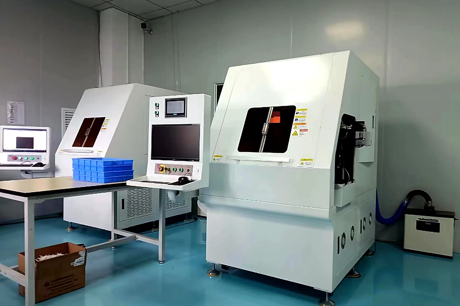
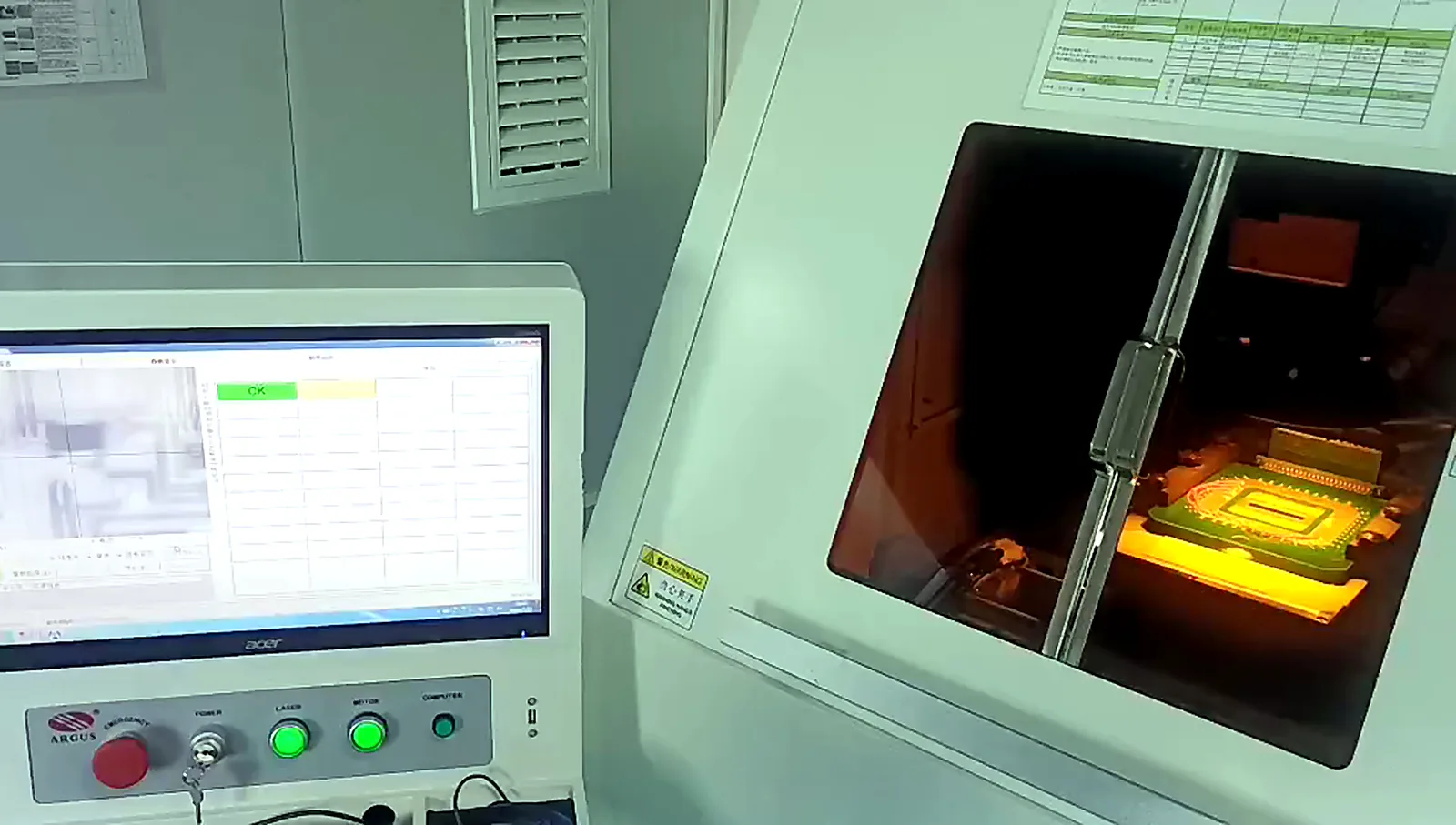
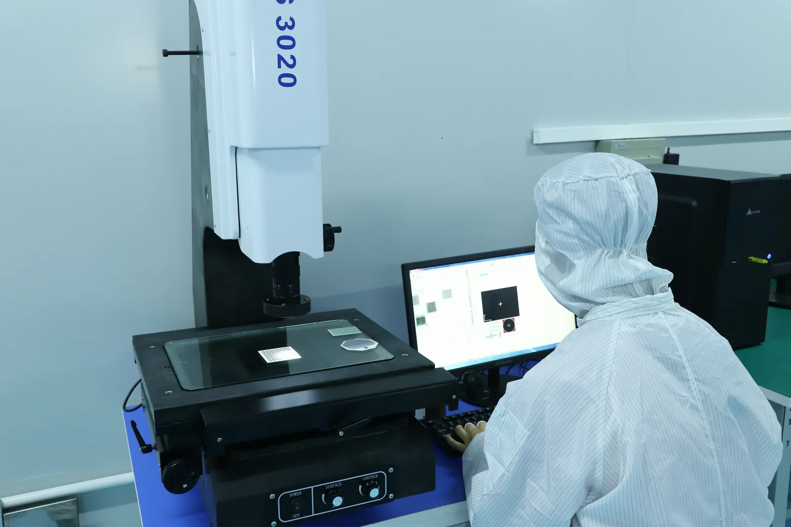
For a critical program, request the equipment route, inspection method, calibration evidence, sample report, and lot-document requirements during RFQ review. Availability is confirmed for the project rather than inferred from a website photograph.
A visual check alone cannot release a functional circuit. The control plan selects measurements and records according to the drawing, application risk, and downstream assembly.
Material identity, drawing revision, outline, thickness, holes, slots, surface condition, flatness or bow where specified, and handling damage.
Coverage, alignment, overlap, edge clearance, pinholes, contamination, conductor condition, resistor geometry, dielectric areas, protection, and trim features.
Continuity, isolation, resistance, ratio, curve, insulation resistance, dielectric withstand, or functional response selected for the product.
Pad or terminal geometry, soldering, bonding, conductive attach, mechanical contact, connector fit, coating windows, and inspection access.
Adhesion, thermal cycling, humidity, media exposure, wear, aging, sample retention, lot records, packaging, and shipment documents when required by project risk.
The exact route changes with the product, but the decision gates remain consistent: define requirements, lock the material and process basis, validate a representative sample, then control revisions and evidence in repeat production.
Confirm the drawing revision, product function, material route, assembly, environment, target volume, and evidence required for release.
Resolve datums, functional geometry, layer stack, paste or ink compatibility, trim allowance, terminals, protection, inspection access, and open assumptions.
Release project-specific artwork, screen or tooling data, process sequence, measurement conditions, sample quantity, and prototype acceptance plan.
Compare visual, dimensional, electrical, thermal, sensor, assembly, and reliability results against agreed requirements. Record deviations before approval.
Lock approved revisions, material and process controls, sampling, traceability, change communication, packaging, and shipment records appropriate to the order.
Attach PDF, Gerber, DXF, DWG, STEP, an electrical table, a thermal or mechanical model, sample photographs, and required inspection records. If a parameter is still unknown, state the application condition so the review can identify the missing decision.