
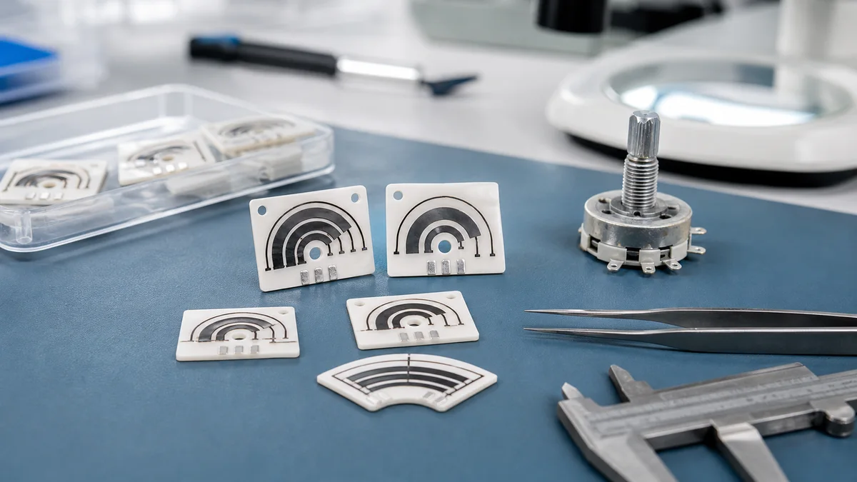
Many potentiometer and sensor projects need a small custom PCB rather than a standard rectangular board. In thick film manufacturing, the substrate may carry the resistive element, terminal pads, collector tracks, solder or spring contact areas, and sometimes a simple signal conditioning layout.
What makes a small sensor PCB different?
The key requirement is not only size. The board must match mechanical movement, contact path, housing, connector, and output curve. This is why arc-shaped ceramic substrates, narrow linear strips, slotted boards, and special mounting hole patterns are common in sensor applications.
Typical functional areas
- Printed resistor track with controlled overlap onto silver end electrodes.
- Separate collector or wiper track with ceramic clearance from the resistor net.
- Terminal pads for soldering, spring contact, welding, bonding, or connector assembly.
- Mounting holes, datum edges, slots, or keyed shapes for the sensor housing.
- Optional protective glass or dielectric areas for wear and insulation control.
Prototype review approach
For a new sensor PCB, it is practical to validate geometry, resistance curve, contact behavior, and assembly fit before committing to larger production tools. A small batch can confirm whether the substrate outline, printed pattern, and terminal design match the real housing.
RFQ checklist
- Existing sample photos or failed legacy part.
- Drawing with outline, holes, slots, and contact path.
- Resistance value or curve across movement range.
- Terminal material and connection method.
- Expected cycle life, contact force, and environmental conditions.