
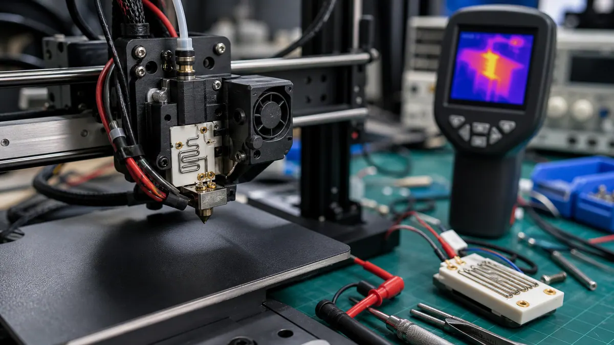
DFM for thick film circuits is different from ordinary FR4 PCB DFM. The design must account for screen printing, paste spreading, drying, firing shrinkage, resistor trimming, dielectric coverage, substrate machining, and inspection method.
Drawing checks
- Confirm substrate outline, holes, slots, corner radius, thickness, and datum references.
- Define conductor width, conductor spacing, terminal pad size, and connection method.
- Show resistor body, silver terminal electrode, and overlap area clearly.
- Separate resistor tracks, collector tracks, and terminals with visible insulation clearance.
- Specify dielectric coverage, protective glass, and any keep-out areas for contact movement.
Process checks
- Screen printing tolerance and paste edge definition.
- Firing profile compatibility between substrate and paste system.
- Layer registration for conductor, resistor, dielectric, and overcoat prints.
- Laser trimming area if trimming is required; omission if the product is designed as non-trimmed.
- Panelization, handling tabs, scribing, cutting, and packaging requirements.
Electrical checks
Include target resistance, tolerance, TCR, output curve, power density, voltage withstand, insulation resistance, continuity, and open/short criteria. For sensor circuits, output versus stroke or angle should be more important than a single resistance value.
Common DFM problems
- Resistor paste touches only the edge of a silver pad instead of overlapping the terminal electrode.
- Collector and resistor tracks are visually too close or ambiguously bridged.
- Mounting holes cut into printed conductors after firing.
- Heater patterns concentrate power in a narrow corner or around a hole.
- Material stack is selected without considering humidity, fuel, oil, or thermal cycling.