
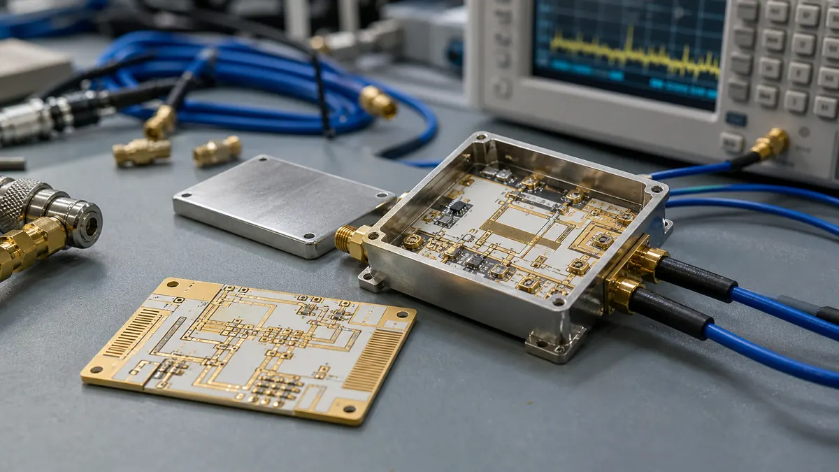
Some thick film ceramic substrates are not finished parts until they are assembled into a hybrid circuit or electronic module. In these projects, the printed ceramic substrate must be designed together with die attach areas, wire bonding pads, solder pads, coating windows, cleanliness needs, and final test requirements.
Chipsimple can review the ceramic circuit side of the interface and help buyers prepare a manufacturable substrate for downstream assembly. The goal is to avoid pad metal mismatch, weak bonding areas, coating conflicts, or thermal stress after the thick film process is complete.
Interfaces to define early
- Die attach pad size, metallization, flatness, and thermal path.
- Wire bonding pad finish, bond area, pull strength requirement, and cleanliness.
- SMT or solder pad geometry, solderability, and reflow temperature exposure.
- Conformal coating, epoxy coating, or protective glass coverage windows.
- Inspection method, functional test points, and traceability marking.
Material and process risks
Conductor paste choice affects soldering, wire bonding, migration risk, adhesion, and cost. Gold, silver-palladium, silver, and other systems should be selected according to the assembly method and environment. If the same pad must support more than one process, the design should be reviewed before tooling.
When hybrid assembly topics appear in RFQ
Keywords such as hybrid assembly, semiconductor packaging, die attach, wire bonding, COB, conformal coating, and high-reliability module usually mean the substrate will be part of a larger assembly. In that case, the drawing package should include both the thick film pattern and the later assembly interface requirements.