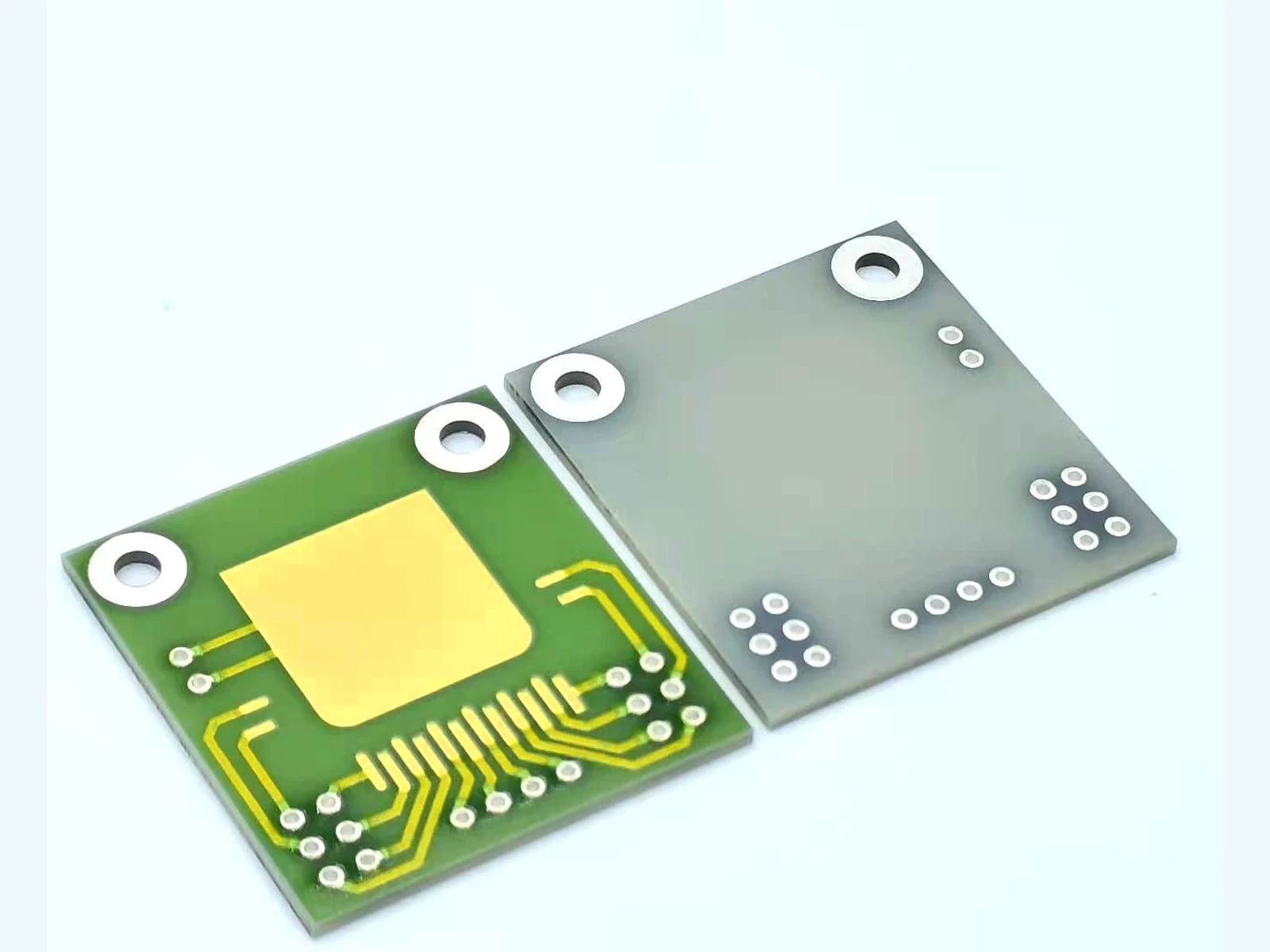
AlN material and heat path
Review grade, thickness, surface, heat sources, interface materials, mounting, cooling boundary, insulation, temperature limits, and assembly-level thermal validation together.

Aluminum Nitride Circuit Engineering
Custom AlN thick film PCBs combine a drawing-selected aluminum nitride substrate with printed routing, pads, protection, and assembly interfaces for thermally demanding electronics. Send the material requirement, artwork, heat sources, cooling boundary, joining method, electrical targets, quantity, and inspection plan so engineering can review the complete route.
Twelve practical selection values cover the ceramic substrate, printed conductor and resistor systems, firing condition, geometry, finish, and dielectric strength.
Final values confirmed against customer drawing.
| Substrate Material | 96% / 99% / 99.6% Alumina / AlN |
|---|---|
| Board Thickness | 0.25–3.0 mm |
| Conductor System | Ag / Ag-Pd / Pt-Ag / Au |
| Resistor System | RuO₂ thick film |
| Conductor Thickness | 10–25 µm typical |
| Resistance Tolerance | ±1% standard (±0.5% available) |
| Firing Temperature | Up to 850°C |
|---|---|
| Thermal Conductivity | ≥24 W/m·K, 96% alumina reference |
| Minimum Line/Space | ≥100 µm |
| Board Size | Max. 120 × 120 mm; larger on request |
| Surface Finish | Bare Ag / ENIG / ENEPIG |
| Dielectric Strength | ≥15 kV/mm |
Four reviews connect the selected AlN material, printed circuit, heat path, assembly, and acceptance plan. Final material properties, numerical performance, joining compatibility, and records remain controlled by approved project documents.
Review grade, thickness, surface, heat sources, interface materials, mounting, cooling boundary, insulation, temperature limits, and assembly-level thermal validation together.
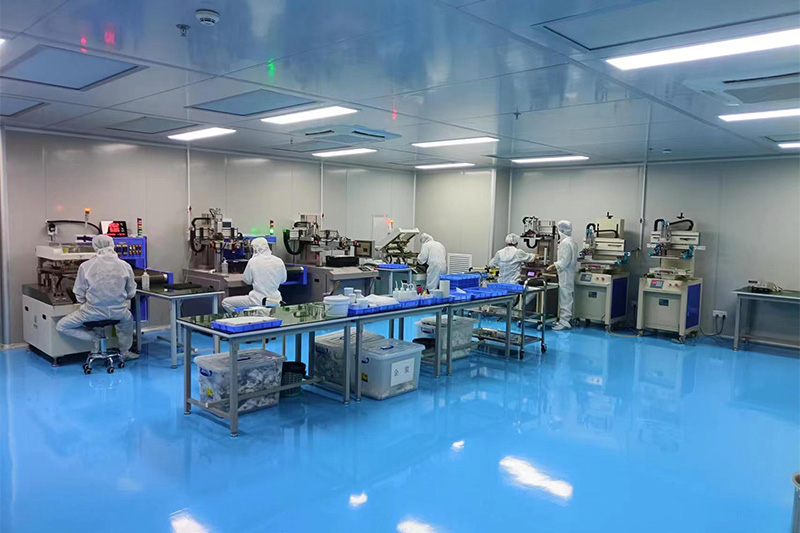
Check line and spacing rules, large pad coverage, openings, keep-outs, common datums, print direction, artwork compensation, and measurable registration criteria.
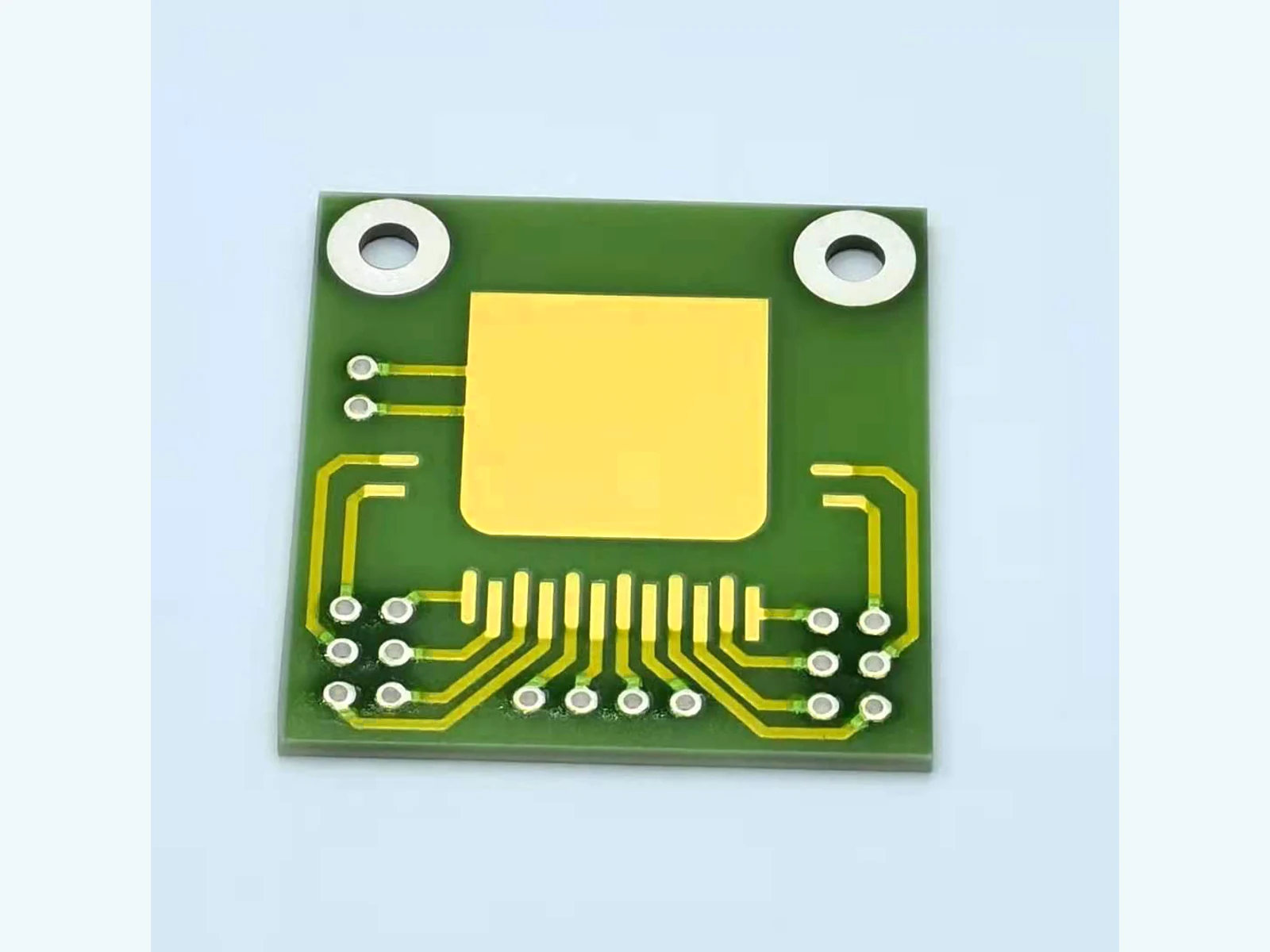
Define pad duty, soldering or bonding route, cleaning, rework, hole purpose, ring construction, front-to-back connection needs, housing, and mechanical loads.
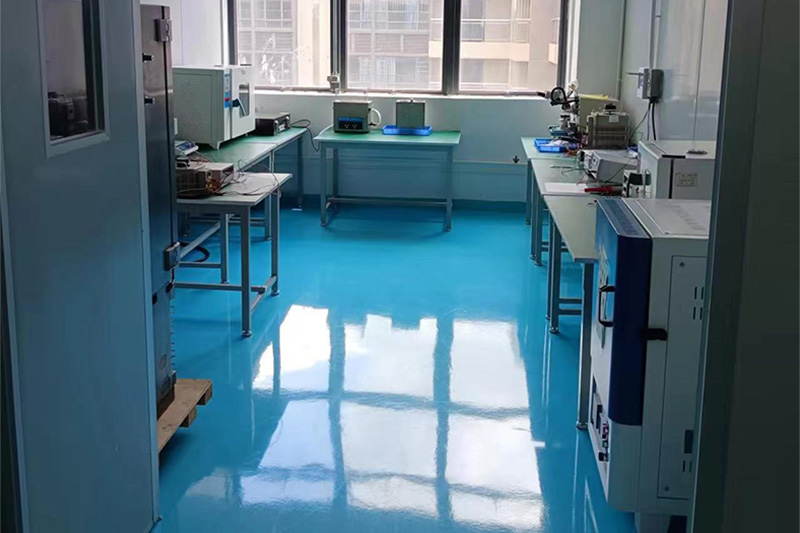
Select visual, dimensional, surface, continuity, isolation, bonding, thermal, traceability, and packing checks with agreed conditions, limits, sampling, and records.
These application directions show where an AlN route may fit after thermal, electrical, mechanical, assembly, environmental, and validation requirements are released.
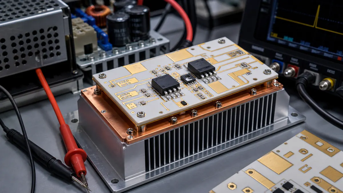 Application illustration
AlN circuits can be evaluated for power assemblies when heat sources, losses, conductor duty, attachment, interface material, cooling boundary, voltage spacing, temperature limits, and validation method are defined.
Review thermal inputs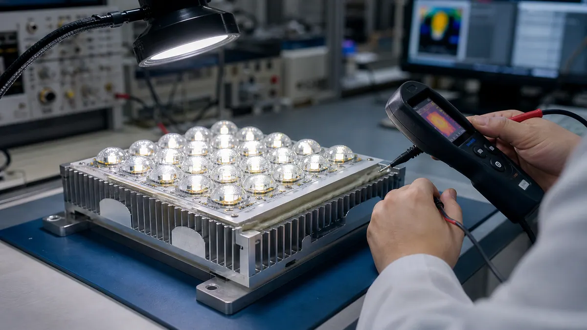 Application illustration
LED assemblies require a complete review of die or package attachment, circuit geometry, optical layout, heat spreading, interface resistance, operating temperature, cycling, insulation, and inspection criteria.
Review LED interfaces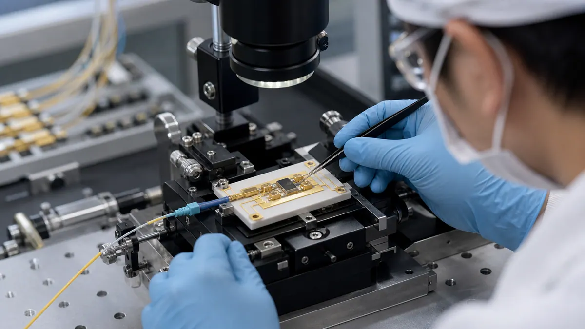 Application illustration
Compact submounts may be reviewed around pad finish, die attach, wire bonding, alignment, optical access, signal integrity, heat flow, cleanliness, rework, and project-specific acceptance tests.
Review submount inputsThe available views show rectangular ceramic parts with gold-colored routing and pads, green coverage, drilled openings, metal-colored rings, and gray rear surfaces in paired and small-group arrangements. They do not establish AlN grade, thermal conductivity, conductor chemistry, hole-wall construction, electrical performance, dimensions, inspection results, lot history, or shipment traceability.
Company resources support thick film screen printing, controlled firing, laboratory inspection, and managed production at the Dongguan site. The applicable AlN material, artwork, thermal route, electrical checks, sampling, traceability, and acceptance records are confirmed for each released project.
View Full Capabilities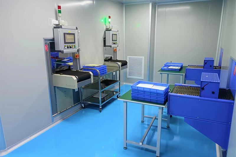
Short answers for quotation planning; released drawings and validation requirements remain controlling.
Send the controlled drawing and artwork, selected AlN grade or required material data, thickness, conductor and pad duty, thermal boundary conditions, joining process, electrical targets, assembly details, inspection criteria, quantity, schedule, and required records. Clear sample photographs can support the first review when CAD data is incomplete.
No single value is presented as a product guarantee. The engineering basis comes from the selected material manufacturer and grade, thickness, surface condition, approved material data, interface layers, mounting, cooling boundary, and the customer's assembly-level model or agreed thermal test.
Color alone cannot answer that question. State the joining process, alloy or wire system, temperatures, cleaning route, pad geometry, required wetting or pull evaluation, rework conditions, and operating environment. Engineering then reviews the conductor or finish system and its project-specific acceptance method.
No. The photographs confirm metal-colored rings around openings, but they do not prove hole-wall metallization, fill, front-to-back continuity, current capacity, isolation, or reliability. Define every aperture function on the drawing and include cross-section, continuity, isolation, or other verification when the design requires it.
Send enough information to connect the selected AlN grade, circuit artwork, thermal path, pad and aperture duties, assembly route, operating conditions, inspection plan, and order scope. Clear sample photographs can begin a review when final CAD data is not ready.
PDF, DWG, DXF, STEP, Gerber, ZIP, Excel, Word, or sample photos are accepted.