
Chipsimple
Ceramic Metallized Thick Film Substrate
Ceramic Metallized Thick Film Substrate for hybrid assembly, packages, sensors, power modules, with alumina, AlN, or zirconia ceramic, fired metallization pads, traces, and terminals, and project-dependent engineering review.
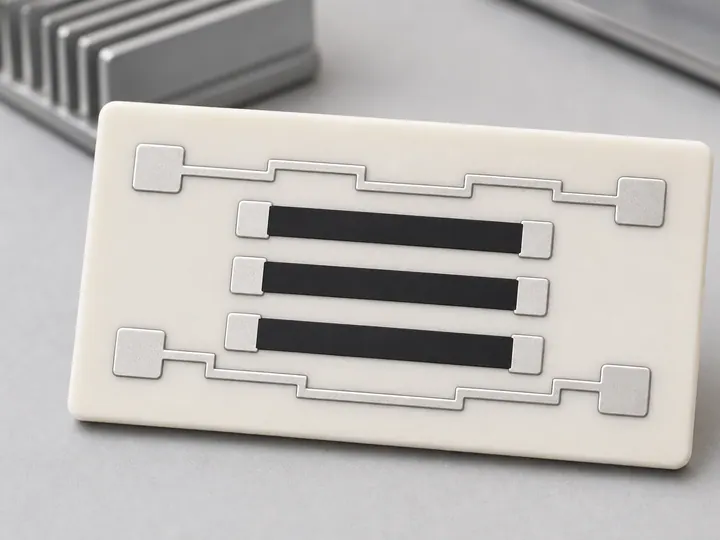
Ceramic Metallized Thick Film Substrate is used when a circuit needs more than standard copper routing: the substrate, printed films, and assembly interface must work as one engineered part.
The usual design review starts with substrate choice, fired metallization pads, traces, and terminals, terminal configuration, electrical targets, operating environment, and inspection method. Chipsimple can review drawings, samples, resistance curves, heating targets, and assembly requirements before prototype or batch planning.
Where this capability fits
This page targets projects involving metallized thick film ceramic substrate on alumina, AlN, or zirconia ceramic. Typical demand comes from hybrid assembly, packages, sensors, power modules where the buyer needs a compact circuit, repeatable electrical behavior, and a manufacturable RFQ package.
Material and process route
| Main substrate route | alumina, AlN, or zirconia ceramic |
|---|---|
| Typical process route | fired metallization pads, traces, and terminals |
| Common project use | hybrid assembly, packages, sensors, power modules |
| Design concerns | adhesion, solderability, metallization stack |
| Production mode | prototype validation, small batch review, and repeat production after requirements are confirmed |
Engineering checks before quotation
- Confirm whether the project needs thick film, thin film, metallized ceramic, DPC, DBC, or another substrate route.
- Provide target resistance, tolerance, TCR, voltage, current, power, thermal load, and any environmental exposure.
- Review conductor finish for soldering, wire bonding, spring contact, connector assembly, or mechanical fastening.
- Define inspection needs such as visual criteria, resistance measurement, insulation resistance, dielectric withstand, adhesion, or functional output.
- Avoid quoting from a photo only when the circuit has a special curve, matched ratio, fine geometry, or reliability requirement.
Design risks to review
The main risks for metallized thick film ceramic substrate are adhesion, solderability, metallization stack. These issues are normally controlled by substrate selection, paste or film system, layout geometry, process control, and a realistic test plan. Exact capability limits remain project-dependent and should be confirmed against the drawing and working conditions.
RFQ data checklist
- Gerber, DXF, DWG, PDF drawing, or clear sample photos with dimensions.
- Substrate material, thickness, outline tolerance, holes, slots, and surface finish.
- Electrical targets including resistance, curve, ratio, TCR, voltage, current, power, and insulation.
- Operating temperature, humidity, chemical exposure, vibration, cleaning, fuel, oil, water, or vacuum conditions.
- Prototype quantity, annual volume, target lead time, packaging, and inspection standard.
Related pages
- Thick Film PCB manufacturing
- Ceramic thick film circuit
- Alumina thick film PCB
- AlN thick film PCB
- Printed thick film resistor
- Thick film manufacturing process
- Thick film resistor design guide
FAQ
Can this page be used as a guaranteed specification?
No. It is an engineering selection guide. Final values depend on material, geometry, process route, test method, and factory confirmation.
When should a buyer send samples?
Samples are useful when the old drawing is incomplete, when a resistance curve must be copied, or when terminal and contact behavior matters.
What is the fastest way to get a useful review?
Send drawings plus operating conditions. For resistor or heater projects, include electrical data and the target test method.