
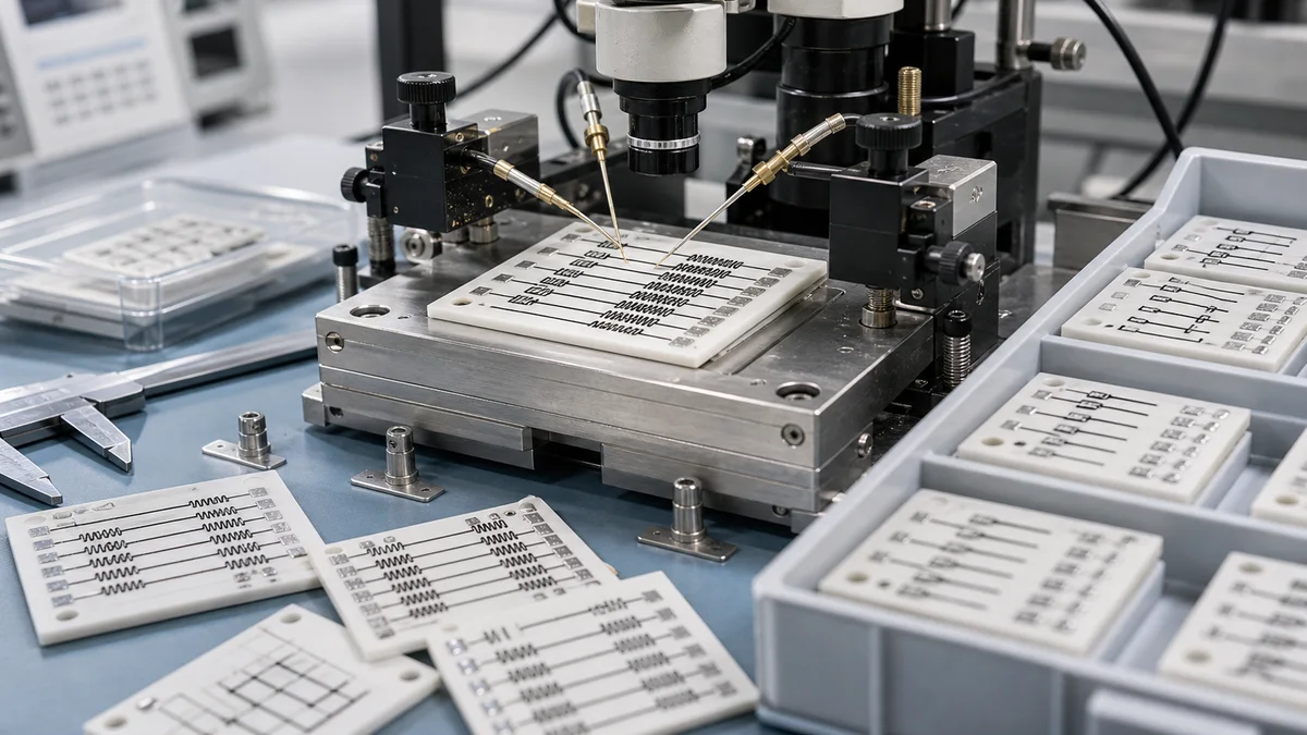
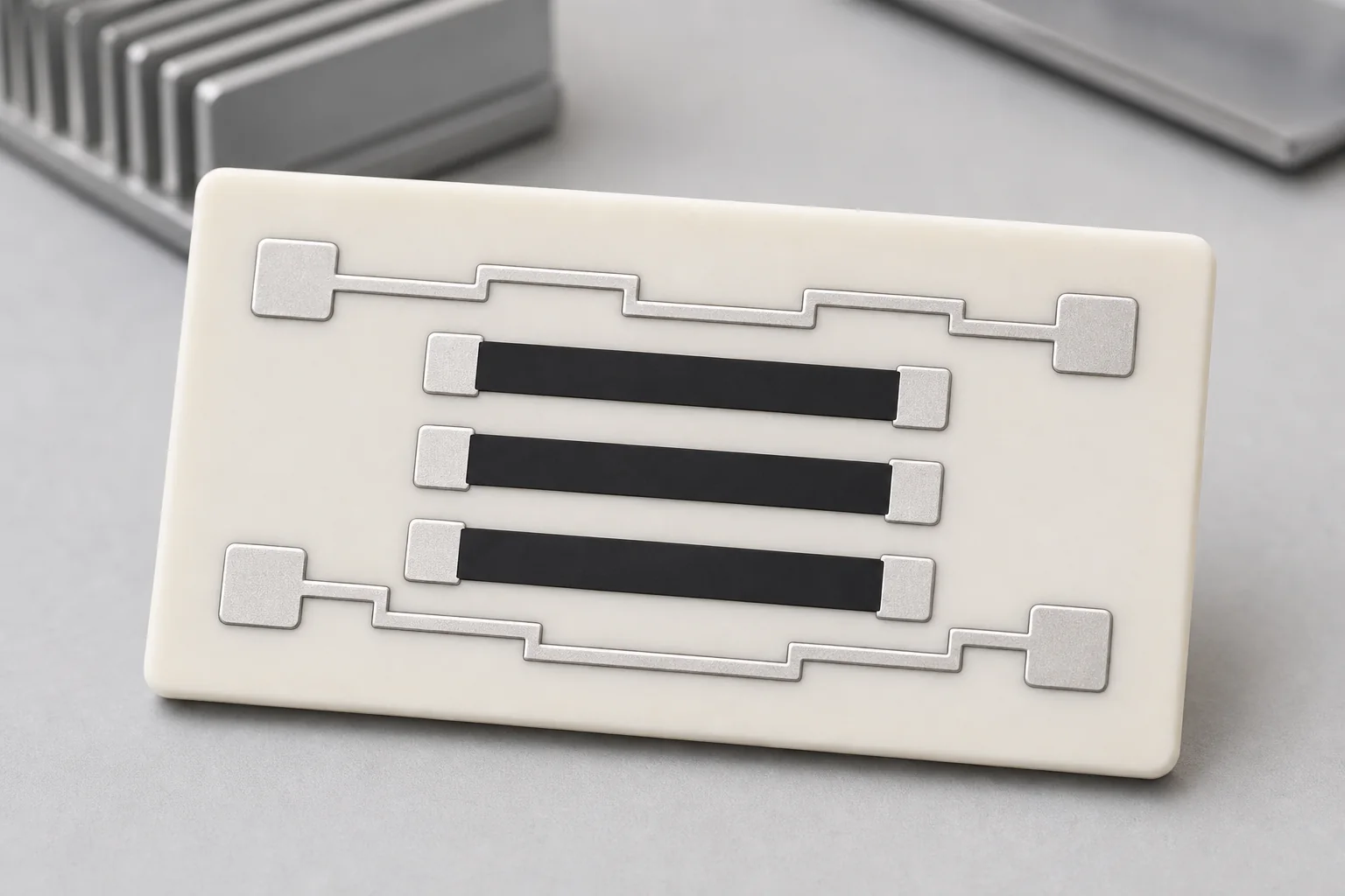
A thick film resistor PCB is selected when the resistance function should be printed directly onto the substrate instead of assembled from separate resistor components. The approach is useful for sensor tracks, resistor networks, custom resistance curves, compact control modules, and products that need stable batch output on ceramic or other high-stability substrates.
Chipsimple reviews each thick film resistor PCB project from the electrical target and the mechanical contact method, not from the drawing alone. The correct route depends on resistor paste, sheet resistance, conductor termination, substrate material, trim allowance, contact wear path, temperature range, and test method.
Where thick film resistor PCB is useful
- Fuel gauge and fuel level sensor resistor cards.
- Throttle position sensor and rotary position sensor tracks.
- Printed resistor networks for compact ceramic circuit modules.
- High-temperature resistor patterns on alumina or AlN substrates.
- Custom resistance curve parts for replacement or new OEM designs.
Design points to confirm
| Design item | Engineering review point |
|---|---|
| Substrate | Alumina, AlN, PI, stainless steel, aluminum substrate, or other project-specific base material. |
| Resistor geometry | Straight, serpentine, arc, ring, multi-track, or custom contact path by drawing. |
| Trimming | Laser trimming allowance, trim path, measurement points, tolerance, and post-trim drift. |
| Contact interface | Wiper path, terminal pad, solder area, spring contact, connector, or mechanical pressure area. |
| Testing | Resistance, curve output, continuity, insulation, visual criteria, adhesion, and environment stress when required. |
RFQ data that improves review quality
For a useful quotation, provide the target resistance range, tolerance, resistance curve table, substrate dimensions, mounting holes, conductor pad design, operating temperature, expected life, quantity, and any existing sample photos. If the product is a replacement part, provide the original output curve and mechanical travel range.