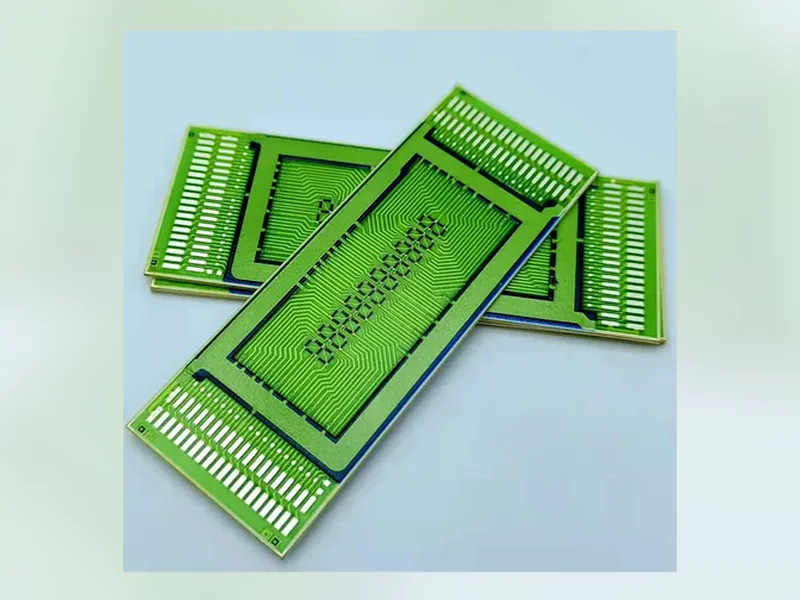
Alumina Thick Film PCB
A balanced fired-ceramic route for printed conductors, resistors, dielectric features, and hybrid assembly interfaces.
Open product page
Ceramic circuit manufacturing route
Printed conductor, resistor, dielectric, crossover, via, and protective layers are reviewed as one fired material stack on alumina or selected aluminum nitride substrates.
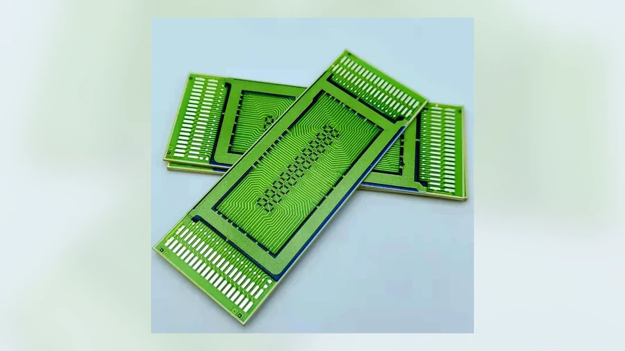
Route definition
Released product pages
Start from the nearest product family, then confirm the drawing, material system, operating conditions, and required evidence.
A balanced fired-ceramic route for printed conductors, resistors, dielectric features, and hybrid assembly interfaces.
Open product page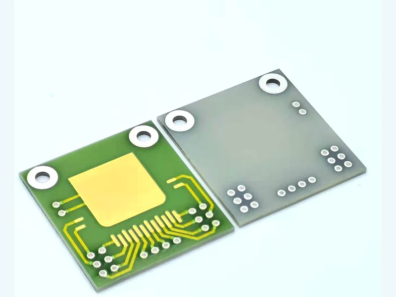
A thermal-management route reviewed around the specified AlN grade, metallization, attachment, and operating condition.
Open product page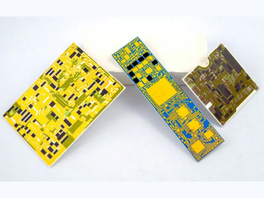
Printed ceramic functions prepared for die, wire, component, terminal, or housing integration.
Open product pageRepeated conductor and dielectric layers for compact routing where the complete firing sequence is compatible.
Open product page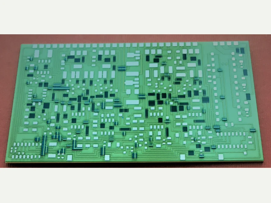
Local insulation and conductor overpasses controlled by overlap, registration, isolation, and test requirements.
Open product pageRFQ checklist
Ceramic material, grade, thickness, outline, holes, slots, and datum scheme
Layer-by-layer artwork and print or firing order
Electrical targets, loading, reference temperature, and test method
Soldering, wire bonding, die attach, terminals, coating, and housing interfaces
Environment, reliability plan, quantity, revision, and traceability needs
Typical programme fit
Suitability and performance are confirmed from the complete assembly and validation conditions, not the application name alone.
Drawing-specific ceramic circuits with printed conductors and, where required, integrated resistors, dielectric crossovers or vias. Bare printed substrates and assembly requirements are quoted as separate scopes.
Send layer artwork, outline and holes, schematic, material preference, electrical limits, assembly method, sample quantity and expected repeat volume.
Send DrawingsCompare crossover count, current paths, thermal exposure, access and inspection before replacing jumper routing with a two-sided ceramic circuit.
Size and validate printed ceramic current paths from processed sheet resistance, geometry, interfaces and thermal boundary conditions.
Sequence die attach, passive placement, wire bonding, cleaning, coating and enclosure steps around access, contamination and rework constraints.
Engineering references