
On this page
- What sheet resistance means
- Why the unit is written Ω/□
- Calculating resistance from the number of squares
- The paste value belongs to a defined fired process
- Why the finished value differs from the ideal calculation
- How sheet resistance should be measured
- Laser trimming must be designed before printing
- Selecting sheet resistance for a real layout
- Information required for design review
Prepared by Chipsimple Engineering Team, Engineering and technical content review
Published online August 9, 2026 · Reviewed August 9, 2026
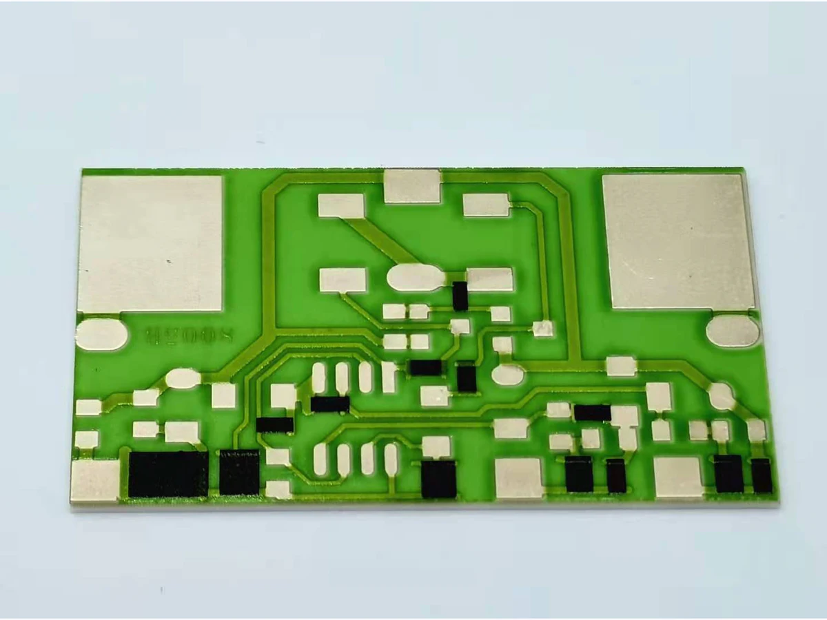
Authorship and scope: This English guide is a technically edited translation of a Chinese article written by a Chipsimple engineer on March 11, 2022. The source screenshot illustration has been replaced with a real product photograph. The equations provide a first-pass design model; production values still depend on the approved paste system, fired process, terminations, substrate, geometry, test conditions, and trim plan.
Sheet resistance is the practical link between a thick film resistor paste and the resistor geometry drawn on a substrate. It allows an engineer to estimate resistance before artwork release, but it is not a stand-alone material constant that can be copied between paste systems or firing conditions. The useful calculation is simple. The discipline lies in defining the conditions behind it.
What sheet resistance means
For a uniform rectangular resistive film with resistivity ρ, length L, width W, and fired thickness t, the ideal resistance between the two opposite end terminations is:
R = ρL / (Wt)
R = Rs × (L/W)
where Rs = ρ/t and N = L/W.
Rs is the sheet resistance and N is the number of squares. When L equals W, the length-to-width ratio is one, so the resistance of the ideal film is equal to its sheet resistance. A 1 mm × 1 mm square and a 10 mm × 10 mm square have the same ideal resistance when the material, fired thickness, uniformity, and edge-contact arrangement are the same.

Why the unit is written Ω/□
Sheet resistance is commonly written as Ω/□, read as “ohms per square.” The square does not add a physical dimension to the ohm. It records the geometric convention: one square of a uniform film has the stated resistance when measured under the defined conditions. Paste data sheets may use “sheet resistance” or “sheet resistivity”; the stated fired thickness, substrate, conductor system, test pattern, firing profile, and measurement conditions determine what the published value means.
This is different from bulk resistivity, whose unit is Ω·m, and from the resistance of a finished printed element, whose unit is Ω. Keeping these terms separate prevents a common drawing error: specifying a paste value as though it were the guaranteed resistance of every printed shape.
Calculating resistance from the number of squares
For a rectangular resistor, divide the effective length by the effective width. Five squares in series give five times the nominal sheet resistance. Parallel geometry requires a current-path analysis rather than simply counting visible blocks.
Worked starting point
| Nominal sheet resistance | 10 kΩ/□ |
|---|---|
| Printed resistor length | 3.0 mm |
| Printed resistor width | 0.6 mm |
| Number of squares | 3.0 / 0.6 = 5 |
| Ideal calculated resistance | 10 kΩ/□ × 5 = 50 kΩ |
The 50 kΩ result is an artwork starting point, not the final production acceptance value. Effective length, termination interaction, the actual fired film, and the measurement method still have to be included in the released design.

The paste value belongs to a defined fired process
Resistor paste is screen printed, dried, and fired to form the functional film. Material suppliers establish typical properties using specified test coupons and processing conditions. Those conditions matter. DuPont's 4300 Series data sheet, for example, ties its resistor system to ceramic substrates, defined print preparation, dried film thickness, and a stated firing route. It also notes that substrate differences can change performance and that print-thickness control is needed for reproducible fired properties.
Film thickness influences resistance, as the basic equation shows, but it should not be treated as an unrestricted correction knob. Changing screen, emulsion, rheology, print setup, drying, or firing can affect more than resistance. It may also change geometry, stability, contact behavior, or the distribution within a lot. If a thickness adjustment is part of the process, it needs a validated window and corresponding inspection control.
Why the finished value differs from the ideal calculation
Several effects separate a production resistor from an ideal rectangle:
- Termination geometry: conductor overlap and the resistor-conductor interface change the effective electrical length and may introduce contact effects.
- Printed-film variation: screen condition, paste rheology, squeegee setup, leveling, and substrate flatness influence deposit geometry and thickness.
- Firing history: furnace profile, loading, atmosphere, and later refiring can shift the resistance distribution.
- Substrate and surface: composition, roughness, cleanliness, and material compatibility affect the fired film.
- Temperature: resistance is stated or measured at a reference temperature; TCR determines how it changes with temperature.
- Current path and loading: corners, narrow regions, trim cuts, and local heat flow can create current crowding or hot spots.
- Protective layers: overglaze or later processing may influence the final value and stability and must be included in validation.
For this reason, engineering release uses an as-fired target and distribution, not only a nominal square count. Representative coupons or parts establish the relationship between artwork and the selected material-process route.
How sheet resistance should be measured
The original illustration shows the essential concept: measure between opposite edges of a square film. In practice, the coupon, conductor terminations, probe locations, applied voltage or current, reference temperature, timing after firing, and instrument method must be defined. The material supplier's test pattern is the correct starting point when verifying a paste data-sheet value.
Lead and contact resistance may be negligible for high-value coupons but material for low-value measurements. A four-terminal method is then considered to separate lead resistance from the film measurement. The chosen method must match the resistance range and the released inspection plan. IEC 60115-1 provides generic terminology, resistance measurement, inspection procedures, and test methods for fixed resistors; the product drawing or detail specification still sets the applicable limits.
Laser trimming must be designed before printing
Laser trimming removes part of the fired resistive path, so it can increase resistance; it cannot lower it. A trimmable design therefore needs an as-fired target below the final value, with enough allowance for the expected distribution but without requiring an excessive cut. The permissible trim ratio, cut style, kerf, stopping method, remaining current path, and post-trim acceptance criteria are established for the geometry and load.

A trim cut changes the current path as well as the measured resistance. Poor placement can concentrate current, reduce effective width, or leave a thermally stressed corner. The design review therefore checks resistor dimensions, conductor overlap, trim access, protective-layer sequence, rated load, and the measurement fixture together.
Selecting sheet resistance for a real layout
The preferred paste decade is not automatically the one closest to the final resistance. Selection considers available area, practical aspect ratio, conductor and overglaze compatibility, firing sequence, target TCR, power density, voltage stress, expected as-fired spread, and trim allowance. A different sheet-resistance grade may produce a more stable geometry even when both options reach the same nominal value mathematically.
Where one paste family does not cover the required range with sensible geometry, a validated blend or another qualified grade may be considered according to the material supplier's guidance. The decision belongs in the approved material and process specification, not as an undocumented shop-floor adjustment.
Information required for design review
- Final resistance or resistance ratios, tolerance, reference temperature, and TCR requirement.
- Operating voltage, current, power, duty cycle, pulse conditions, and permissible temperature rise.
- Substrate material, grade, thickness, outline, surface condition, and available resistor area.
- Conductor, resistor, dielectric, overglaze, and terminal stack, including the firing sequence.
- Artwork dimensions, minimum clearances, termination overlap, trim access, and keep-out areas.
- As-fired window, final trim target, test method, reference conditions, and required records.
- Assembly operations, environmental exposure, qualification tests, quantities, and drawing revision.
Sheet resistance makes the first calculation possible. A releasable resistor design comes from connecting that calculation to the real fired film, current path, trim strategy, electrical load, and inspection method.
Primary references
- DuPont, 4300 Series Resistors technical data sheet — paste-specific sheet-resistance range, substrate, printing, dried-film, firing, and process-control context.
- IEC 60115-1:2020, Fixed resistors for use in electronic equipment — Part 1 — generic terminology, resistance measurement, inspection procedures, and test methods.
Review a resistor layout before artwork release
Send the resistance target, load, substrate, available geometry, layer stack, trim requirement, environment, quantity, and inspection needs. Existing samples and measured data are useful when the project is a replacement.