
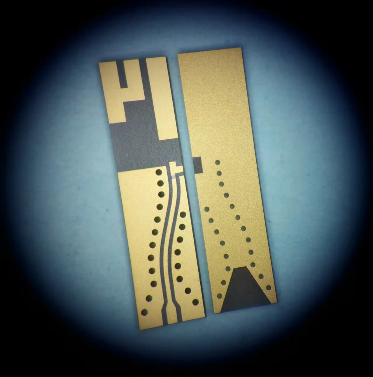
Overview
This product selection record defines a drawing-led selection boundary for Thin Film Ceramic Circuits. It separates the requested construction from adjacent routes and identifies material, geometry, interface, inspection, and supply evidence needed before quotation or publication.
Engineering review matrix
Each row links a design variable to evidence that can support a drawing or release decision.
| Variable | Control question | Verification route |
|---|---|---|
| Material identity | For Thin Film Ceramic Circuits, ceramic chemistry, grade, source data, lot, thickness, surface, and thermal/mechanical properties must match the actual route. | Review source documentation and incoming measurements within stated scope. |
| Mechanical geometry | Outline, thickness, flatness, bow, holes, slots, edge, datum, scribe, and break direction affect printing and assembly. | Measure with a drawing-linked datum and brittle-part method. |
| Surface condition | Roughness, cleanliness, porosity, lapping, polishing, and handling influence print definition, adhesion, deposition, and bonding. | Inspect the controlled surface before metallization or printing. |
| Thermal interface | Conductivity values belong to a named grade and temperature; assembly interfaces and geometry control real heat flow. | Use source data for selection and assembly-level thermal validation for release. |
| Metallization compatibility | Paste, deposited metal, adhesion layer, firing, plating, soldering, and wire bonding need route-specific compatibility. | Qualify the complete material and assembly stack rather than the bare substrate alone. |
Selection route
The order makes assumptions and ownership visible before a result is promoted to a requirement.
- 01
Define the functional job
For Thin Film Ceramic Circuits, document the functional requirement, operating boundary, interfaces, quantities, and acceptance owner against the current drawing.
- 02
Separate adjacent process routes
For Thin Film Ceramic Circuits, compare the applicable material and process routes, recording compatibility limits, trade-offs, and verification needs before selection.
- 03
Release geometry and interfaces
For Thin Film Ceramic Circuits, control dimensions, datums, layer stack, interfaces, tolerances, and assembly constraints in the released drawing.
- 04
Agree inspection evidence
For Thin Film Ceramic Circuits, agree the inspection method, sample plan, acceptance criteria, traceability, and report format before validation.
- 05
Quote against the controlled drawing
For Thin Film Ceramic Circuits, control dimensions, datums, layer stack, interfaces, tolerances, and assembly constraints in the released drawing.
Failure controls
These are review prompts, not evidence that every risk applies or that every test is available.
- A
Cracking or chipping from machining, handling, mounting, or thermal stress
- B
Registration or bonding loss from surface, flatness, or cleanliness variation
- C
Thermal performance assumed from generic values rather than actual grade and assembly
- D
Metallization adhesion or interface failure after processing and exposure
Inputs for a practical review
Unknown values may be labelled unknown. The review should convert uncertainty into an explicit decision or validation task.
Send Drawings- 01
Ceramic family, grade, source document, and lot requirement
- 02
Outline, thickness, flatness, holes, slots, scribe, and edge tolerances
- 03
Surface finish, cleanliness, lapping/polishing, and protected faces
- 04
Metallization/printing, joining, mounting, and heat-path requirements
- 05
Incoming, dimensional, adhesion, thermal, and reliability evidence