Hybrid interconnect and resistor functions
Ceramic circuits may integrate pads, resistors, bias networks, heaters, or sensor interfaces when the metallization and assembly route are compatible.

Application engineering guide
Define frequency or precision behavior, material data, geometry, grounding, optical or RF alignment, assembly, cleanliness, thermal drift, and test fixtures together.
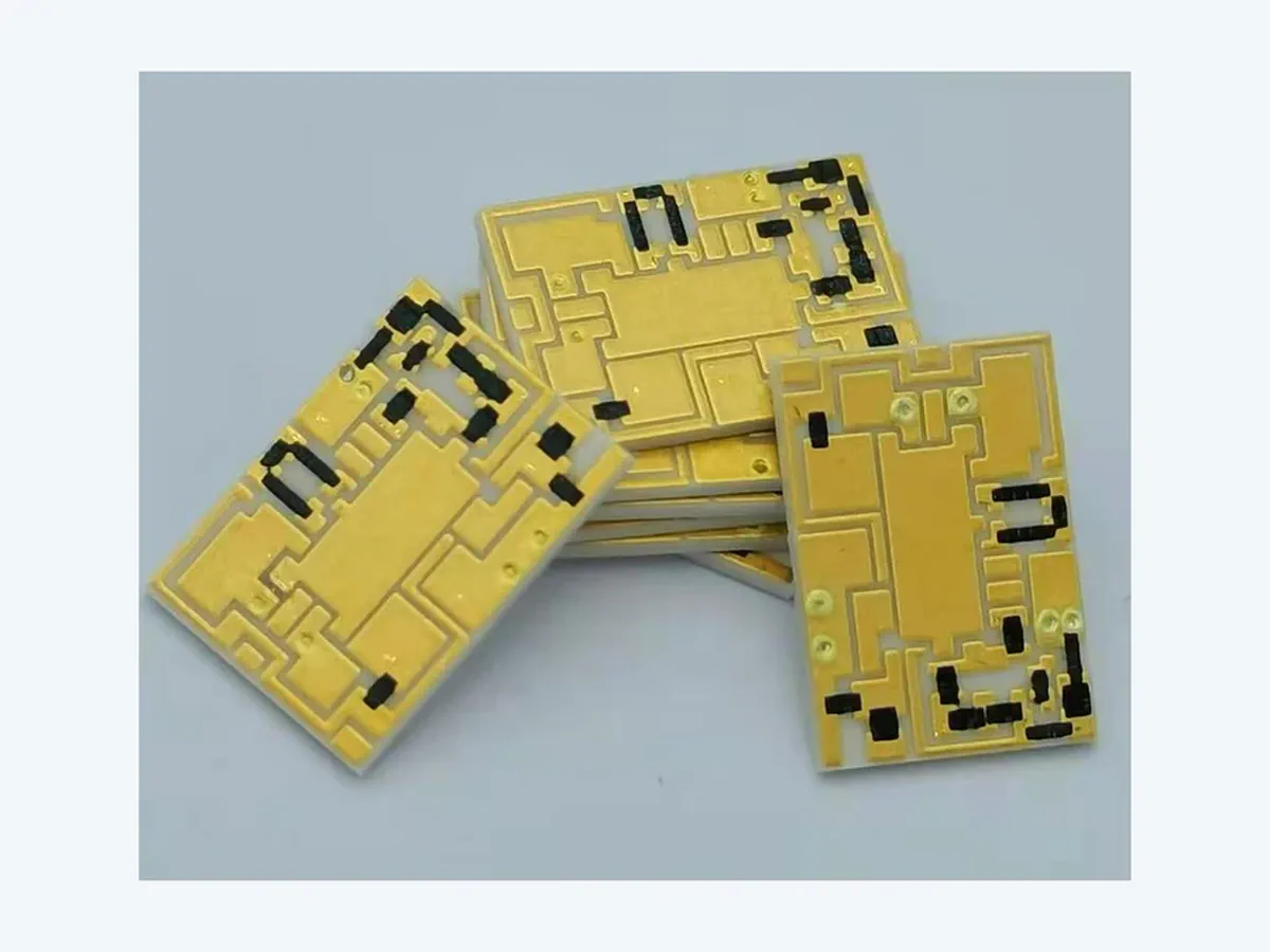
RF, photonic, and precision-instrument modules are sensitive to more than nominal conductivity or resistor value. Substrate data, line geometry, grounding, surface finish, attachment, bond-wire transitions, optical alignment, cleanliness, thermal drift, enclosure modes, and the measurement fixture can all change the result.
Classic thick film may suit some interconnect, resistor, heater, or hybrid functions. Thin film or another ceramic process may be needed for finer geometry or RF performance. The routes must not be combined into one generic ceramic-PCB claim.
Ceramic circuits may integrate pads, resistors, bias networks, heaters, or sensor interfaces when the metallization and assembly route are compatible.
Local heating or temperature sensing may support wavelength or detector stability after the optical mount, sensor location, heat path, control loop, and drift limits are defined.
Line geometry, reference planes, vias, cavity, connector launch, bonding, material properties, and surface finish must be analysed as a complete transition.
Ratios, tracking, loading, leakage, guarding, shielding, temperature, calibration, and cleanliness can be more important than the nominal resistor values.
The test fixture and assembly are part of the electrical result. Release them with the circuit instead of treating the ceramic as an isolated coupon.
| System requirement | Why it changes the circuit | What the project must define |
|---|---|---|
| Frequency or precision target | Sets geometry, material-property controls, resistor technology, parasitic budget, shielding, grounding, and test access. | Frequency band or accuracy budget, impedance, loss, phase, ratio, noise, drift, loading, and acceptance limits. |
| Material and geometry | Influences dielectric behavior, line dimensions, conductor system, surface, thickness, flatness, vias, and thermal expansion. | Material grade and data source, thickness, surface condition, outline, holes, line data, tolerances, and lot controls. |
| Optical or RF transition | Controls connector launch, bond wires, cavity, fiber or laser alignment, thermal interface, grounding, and mechanical datums. | 3D assembly, launch or optical model, bond diagram, datums, alignment budget, torque, and interface materials. |
| Assembly and cleanliness | Determines finish, die attach, solder, wire bonding, cleaning, outgassing, coating, handling, packaging, and rework. | Process materials and temperatures, cleanliness criteria, allowable residues, bond tests, storage, and handling class. |
| Measurement correlation | Requires controlled fixtures, calibration planes, probe pads, de-embedding, environmental control, and traceable equipment. | Fixture drawings, calibration method, reference plane, cables or probes, temperature, sampling, and raw-data format. |
A credible application page should make the surrounding interfaces visible. These are the places where otherwise reasonable component designs often fail during integration.
Coupon data can inform design, but final RF, optical, or precision performance should be measured in the released fixture and production-intent module.
Verify dimensions, surface condition, metallization, resistor values, cleanliness, attachment, bonding, and alignment datums.
Expected outputTraceable visual, dimensional, and electrical baseline.
Establish calibration planes and compare coupon, bare substrate, and assembled module behavior where relevant.
Expected outputFixture loss or offset, de-embedding method, and repeatability record.
Measure RF, optical, thermal, or precision performance across the defined frequency, temperature, power, and loading envelope.
Expected outputPlots and raw data tied to the assembly revision and test method.
Apply thermal cycling, humidity, storage, vibration, power, aging, or cleanliness stress required by the program.
Expected outputPre/post functional comparison and physical-interface inspection.
Mark unknown values as “for application review.” The first response is more useful when the system interfaces and validation responsibility are visible from the start.
Upload drawings, a requirements file, or clear sample and assembly photos.
Short answers to scope questions that often block a useful quotation.
No. Some functions may suit thick film, while fine geometry, loss, frequency, finish, or tolerance requirements may point to thin film or another process. The design and test plan should determine the route.
Connectors, launches, cables, probes, calibration planes, cavity geometry, and de-embedding can materially affect measured performance. Without the fixture definition, circuit and measurement errors are difficult to separate.
No. It is a generated application visualization used to explain assembly context. Customer-project proof requires authorized, traceable product, process, and test evidence.