Gate-drive and sensing interface
A compact ceramic circuit may support driver interconnect, sensing, bias, or protection components when isolation, switching noise, attachment, and inspection are defined.

Application engineering guide
Connect electrical waveforms, isolation, heat flow, power-module assembly, transients, cooling, and fault behavior before choosing a ceramic substrate.
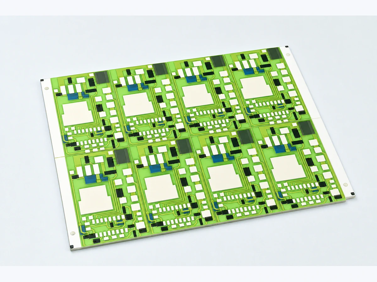
A ceramic circuit near a power stage may handle sensing, biasing, gate-drive interconnect, discharge, balancing, or local control. Each function brings different voltage waveforms, current, isolation, heat, switching noise, attachment, cooling, and fault requirements. Material selection should follow the released electrical and thermal architecture.
Thick film, thin film, DPC, DBC, and AMB are different processes. This guide focuses on deciding whether a printed ceramic circuit function is appropriate before any specific manufacturing route is released.
A compact ceramic circuit may support driver interconnect, sensing, bias, or protection components when isolation, switching noise, attachment, and inspection are defined.
Voltage sensing, discharge, balancing, limiting, or damping may use printed resistors only after continuous, pulse, surge, energy, ratio, loading, and heat-removal conditions are supplied.
Alumina or AlN may be reviewed where heat spreading, electrical insulation, dimensions, and assembly compatibility matter, but material data and thermal modelling must match the project.
Die attach, wire bonding, soldering, conductive adhesive, coating, and connector interfaces can drive metallization and cleanliness requirements as strongly as the base ceramic.
Do not select a ceramic route from a generic thermal-conductivity number. Use the actual stack, interfaces, waveforms, cooling, and qualification plan.
| System requirement | Why it changes the circuit | What the project must define |
|---|---|---|
| Electrical waveform | Defines resistor loading, conductor current, isolation, clearances, parasitic sensitivity, pulse energy, and measurement approach. | Continuous, pulse and surge voltage or current, frequency, duty, source impedance, load, duration, repetition, and faults. |
| Thermal path | Controls ceramic choice, thickness, metallization, attachment, spreader, interface pressure, cooling, temperature gradients, and cycling stress. | Loss map, junction or component limits, coolant or airflow, heat-sink flatness, interface material, clamp load, and ambient profile. |
| Isolation environment | Affects spacing, dielectric or barrier strategy, surface condition, coating, pollution, altitude, and test voltage. | Working and transient voltage, insulation coordination, pollution degree, altitude, grounding, creepage path, and safety standard. |
| Assembly process | Determines pad metallurgy, solder or attach system, wire-bond areas, reflow or cure exposure, cleaning, planarity, and repair policy. | Process temperatures, alloys or adhesives, bond wire, component sizes, cleaning, coating, inspection, and allowable rework. |
| Fault and qualification | May require derating, redundant sensing, thermal shutdown, traceability, cycling, vibration, overload, and destructive analysis. | Fault cases, protection timing, mission profile, qualification matrix, sampling, records, and change control. |
A credible application page should make the surrounding interfaces visible. These are the places where otherwise reasonable component designs often fail during integration.
Power-electronics validation must use production-intent mounting, cooling, switching, and fault conditions. Bench resistance or insulation measurements are necessary but not sufficient.
Confirm geometry, pad condition, attachment, bond or solder quality, resistance, continuity, isolation, and dimensional stack.
Expected outputReleased pre-power inspection record.
Evaluate waveforms, loading, sensing accuracy, switching behavior, temperatures, and control stability at representative operating points.
Expected outputElectrical and thermal correlation under defined cooling.
Apply defined surges, pulses, overloads, temperature swings, power cycling, vibration, humidity, or altitude conditions.
Expected outputPre/during/post functional data and interface inspection.
Test the specified open, short, cooling loss, gate fault, sensor fault, or overload cases in the protected assembly.
Expected outputFault response and qualification evidence owned by the system program.
Mark unknown values as “for application review.” The first response is more useful when the system interfaces and validation responsibility are visible from the start.
Upload drawings, a requirements file, or clear sample and assembly photos.
Short answers to scope questions that often block a useful quotation.
No. AlN can offer a higher-conductivity route, but cost, surface, thickness, metallization, attachment, insulation, flatness, mechanical stress, availability, and the complete thermal stack must be reviewed together.
No. They use different material and metallization routes and support different geometry, copper or film thickness, assembly, and reliability needs. The project architecture should determine the route.
Provide continuous and transient voltage, current, pulse width, repetition, energy, duty, source impedance, cooling, mounting, ambient, overload, and fault conditions—not only nominal resistance and wattage.