
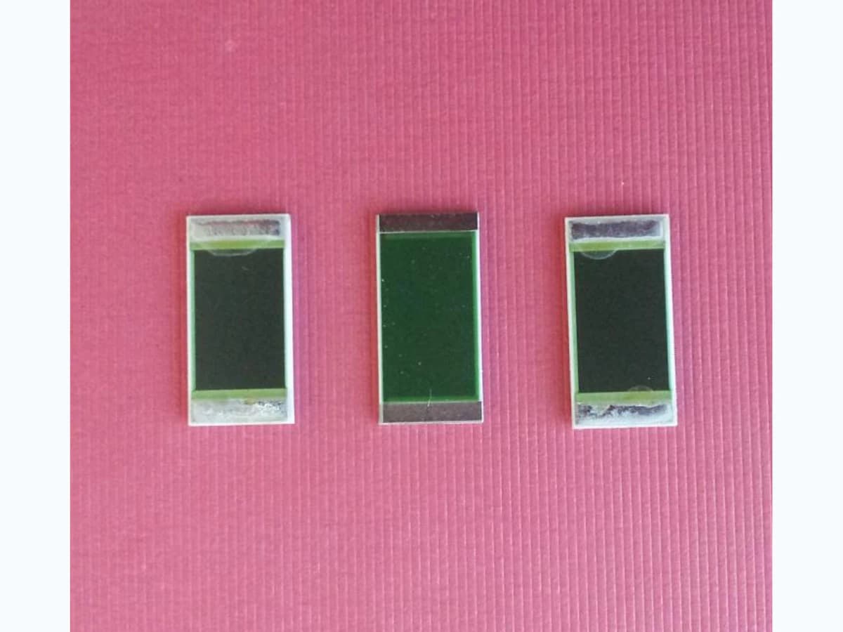
Overview
Printed-resistor power density is a useful screening quantity only when its area, resistance state, duty, heat path, and temperature criterion are explicit. A nominal resistor can dissipate the same electrical power in very different thermal conditions depending on substrate thickness, nearby conductors, termination geometry, overglaze, mounting, airflow, enclosure, and neighboring heat sources. Derating therefore means reducing allowed electrical stress as one or more boundary conditions become less favorable; it is not a universal percentage copied from a component catalog. The design must connect local film loading to measured resistor temperature, resistance shift, substrate stress, and the finished assembly's acceptance plan.
Engineering review matrix
Each row links a design variable to evidence that can support a drawing or release decision.
| Variable | Control question | Verification route |
|---|---|---|
| Element power and waveform | Define RMS and peak voltage and current, duration, repetition, startup, overload, source impedance, current limit, and simultaneous loading of neighboring elements. | Record synchronized electrical waveforms at nominal and worst credible states and calculate power with the appropriate time basis. |
| Resistor geometry | Control fired width, length, aspect ratio, thickness observation, corners, conductor overlap, trim allowance, cut geometry, and distance to edges or other heat sources. | Inspect drawing-linked features and correlate geometry with element resistance and thermal maps across representative positions. |
| Material and process history | Name resistor and conductor families, substrate, protection, print sequence, drying, firing, refires, trim, cleaning, and assembly heat without transferring supplier typical data. | Retain lot and process records and compare coupons or representative product data before and after downstream processing. |
| Thermal interfaces | Specify interface material, bond-line or gap, contact area, pressure, flatness, fasteners, heat sink, heated load, airflow or fluid, and enclosure boundary. | Measure or bound interface behavior and correlate model predictions with the production-intent mounted assembly. |
| Temperature criterion | Define ambient, local film proxy, substrate, terminal, load, enclosure, and nearby-component limits with sensor type, location, emissivity treatment, and stabilization rule. | Use fixed drawing-referenced measurement locations and document sensor attachment, calibration, uncertainty, and spatial resolution. |
| Electrical side effects | Allocate TCR, voltage coefficient, noise, leakage, insulation, parasitic paths, contact resistance, and ratio tracking alongside the thermal budget. | Measure electrical response under the same powered temperature states rather than extrapolating low-level room-temperature readings. |
| Exposure and stability | Define cycling, dwell, humidity, contamination, media, vibration, assembly stress, storage, aging, acceptable resistance shift, and failure criteria. | Compare pre-, intermediate-, and post-exposure measurements with visual and microscopic inspection under a controlled data plan. |
Controlled model
Electrical loading and thermal derating model
Start with the exact resistor body and thermal boundary. Area-based loading, lumped thermal resistance, and temperature coefficients can screen a design, but a printed film is neither an ideal uniform sheet nor an isolated catalog resistor. Termination overlap, trim cuts, temperature gradients, protection, adjacent conductors, and substrate stress can dominate local behavior.
P = I²R = V²/RCalculates electrical power in a resistor for a defined voltage, current, and resistance state.
- Units
- P in W; I in A; V in V; R in Ω
- Use boundary
- Use the actual waveform and resistance at the relevant temperature. Pulses, startup, controller modulation, source impedance, and abnormal states require time-resolved treatment.
p_A = P / A_fDefines average electrical power per designed fired resistor area.
- Units
- p_A in W/mm² or W/cm²; P in W; A_f in matching area units
- Use boundary
- Average film-area loading does not identify local peaks at corners, terminations, trim cuts, thickness changes, or unequal cooling.
ΔT ≈ P θ_thScreens steady temperature rise above a defined reference through a lumped thermal resistance.
- Units
- ΔT in K; P in W; θ_th in K/W
- Use boundary
- Valid only for a stated steady boundary. Thermal resistance changes with mounting, interfaces, airflow, fluid, radiation, temperature, and contact quality; transient response needs thermal capacitance.
R(T) ≈ R_ref [1 + α(T − T_ref)]First-order estimate of resistance change with temperature near a reference condition.
- Units
- R in Ω; α in 1/K or ppm/K; T in °C or K differences
- Use boundary
- Use only over a validated interval for the named material and geometry. It does not cover nonlinear TCR, voltage coefficient, self-heating gradients, hysteresis, or aging.
Decision comparison
| Decision | Route A | Route B | Verification |
|---|---|---|---|
| Average power versus local stress | Total or average-area power is convenient for early sizing and comparing layouts at a common boundary. | Local current density and heat removal near terminations, trim cuts, corners, or partial contact determine the most stressed film region. | Correlate electrical data with fine-location temperature mapping and post-stress inspection on the actual geometry rather than approving from average power alone. |
| Continuous duty versus pulses | Long steady operation approaches an assembly-specific equilibrium controlled by heat paths and ambient losses. | Short pulses depend on energy, film and substrate heat capacity, pulse spacing, peak voltage or current, and cumulative baseline heating. | Capture time-resolved voltage, current, and temperature or resistance response for the complete waveform, including startup and repetition. |
| Free-air coupon versus mounted assembly | A coupon isolates material and process variables and can support screening or correlation. | The product mounting stack adds clamps, adhesives, interfaces, enclosure, neighboring sources, airflow, fluid, and mechanical stress. | Use coupons for process understanding but qualify the released resistor in a production-intent assembly across the specified environments. |
- Voltage coefficient, electric-field concentration, and insulation spacing can govern before average thermal loading does, especially in high-value or high-voltage elements.
- A firing-process temperature from a material data sheet is not an operating-temperature limit for the printed resistor or assembly.
Power-derating workflow
The order makes assumptions and ownership visible before a result is promoted to a requirement.
- 01
Define the resistance function
Document nominal value, tolerance, reference temperature, TCR or tracking needs, voltage coefficient concerns, noise and stability criteria, circuit topology, source and load, and whether initial trim or system calibration is allowed. Make the element-level electrical states visible instead of quoting only total network power.
- 02
Describe every load state
Provide continuous, startup, pulse, overload, standby, reverse, transient, and fault waveforms with duty and repetition. Calculate voltage, current, power, and energy at resistance and supply extremes; retain controller behavior, source impedance, and current limiting as explicit assumptions.
- 03
Map local geometry and materials
Identify fired resistor length, width, thickness observation, conductor overlap, corner style, trim cuts, overglaze, nearby layers, substrate outline, holes, and edges. Review local current paths and thermal sinks rather than dividing total power by the whole ceramic area.
- 04
Build the assembly heat path
Model heat flow through substrate, printed layers, interfaces, fasteners, adhesive or grease, housing, fluid or airflow, radiation, neighboring components, and insulation. Include tolerance cases for contact pressure, bond-line thickness, contamination, and partial mounting contact.
- 05
Design a validation matrix
Specify measurement locations, resistance reference, instrument loading, waveform capture, temperature method, stabilization, cycling, humidity or chemical exposure, mechanical state, sample selection, and post-test inspection. Keep qualification conditions distinct from routine outgoing inspection.
- 06
Issue bounded derating rules
Translate correlated evidence into a project-specific curve, table, or prohibited-state map with margin and uncertainty. Tie it to drawing revision, material stack, process window, mounting, controller, environment, and change control so a later substitution cannot inherit the result automatically.
Failure controls
These are review prompts, not evidence that every risk applies or that every test is available.
- A
Publishing a generic watt-per-area value as a product rating without naming film area, material, geometry, mounting, ambient, waveform, and temperature criterion.
- B
Averaging power over a resistor while ignoring local hot regions at narrow sections, trim cuts, conductor overlaps, turns, and thermally isolated edges.
- C
Validating a free-air sample, then using the result after changing the interface, clamp, housing, enclosure, airflow, fluid, or nearby heat sources.
- D
Applying a steady-state derating curve to pulses or controller waveforms whose peak voltage, energy, repetition, and cumulative heating were not tested.
- E
Treating initial resistance stability as proof of long-term behavior despite protection, assembly heat, humidity, bias, cycling, or mechanical stress.
- F
Using supplier typical coupon values as guaranteed outgoing limits or as evidence of ChipSimple material selection and production control.
Reference boundary
Public method sources
These sources support the engineering method and terminology used in this technical guide. They do not establish a ThickFilmPCB material list, capability limit, customer result, certification, or finished-product specification.
- 01IEC 60115-1:2020 — Fixed resistors for use in electronic equipment
Supports fixed-resistor terminology, ratings, preferred characteristics, test and measurement concepts, and the need to state conditions. The standard does not provide a universal printed-resistor power density or prove any ChipSimple rating.
- 02Heraeus — R8900 Series air-fired resistor system technical data sheet
Supports treating sheet resistance, geometry, termination, firing, TCR, voltage behavior, and test conditions as linked for one named material family only; its typical values are not transferable capability or derating evidence.
- 03Vishay — Basics of Linear Fixed Resistors
Provides manufacturer-authored terminology for rated dissipation, temperature rise, ambient derating, pulse loading, voltage limitation, and resistor temperature only. It is not thick-film process evidence and establishes no ChipSimple limit.
- 04NIST Technical Note 1297 — measurement uncertainty
Supports an explicit uncertainty budget for electrical, dimensional, and temperature measurements used to establish a project envelope; it supplies no resistor rating or acceptance value.
Inputs for a practical review
Unknown values may be labelled unknown. The review should convert uncertainty into an explicit decision or validation task.
Send Drawings- 01
Circuit schematic and element table with nominal values, tolerances, node voltages, current, power, simultaneous loads, and calibration strategy.
- 02
Complete voltage and current waveforms including startup, pulse duration and repetition, standby, overload, transients, current limiting, and fault states.
- 03
Fired resistor artwork and dimensions, conductor overlaps, trim locations, layer stack, substrate geometry, holes, edge clearances, and protection.
- 04
Mounting and heat-path details including housing, interface, contact pressure, fasteners, load, enclosure, airflow or fluid, insulation, and neighboring sources.
- 05
Ambient and local temperature requirements, measurement locations and methods, warm-up, stabilization, cycling, and permissible gradients.
- 06
Electrical stability, TCR, VCR, noise, leakage, isolation, resistance-shift, environmental, mechanical, and life-related acceptance criteria.
- 07
Prototype quantities, tolerance samples, validation matrix, sampling, data deliverables, traceability, drawing revision, substitutions, and change-control rules.