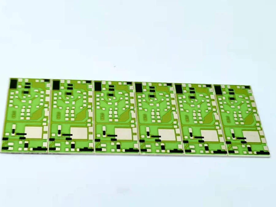
Printed Thick Film Resistor
Custom resistor geometry reviewed with paste system, terminations, load, protection, and measurement method.
Open product page
Printed resistor manufacturing route
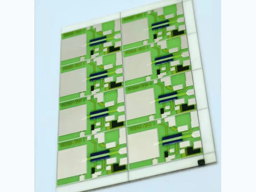
Resistance is designed from paste family, effective geometry, terminations, fired process, electrical load, protection, measurement conditions, and—where required—a planned laser-trim path.
Route definition
Released product pages
Start from the nearest product family, then confirm the drawing, material system, operating conditions, and required evidence.
Custom resistor geometry reviewed with paste system, terminations, load, protection, and measurement method.
Open product page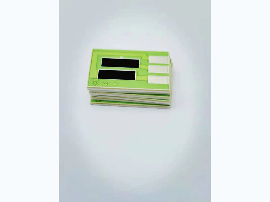
Printed resistor elements and conductor interfaces on a released ceramic layout.
Open product page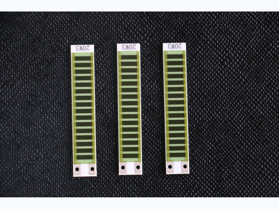
Multiple values or ratios integrated into one ceramic part with a shared trim and inspection strategy.
Open product page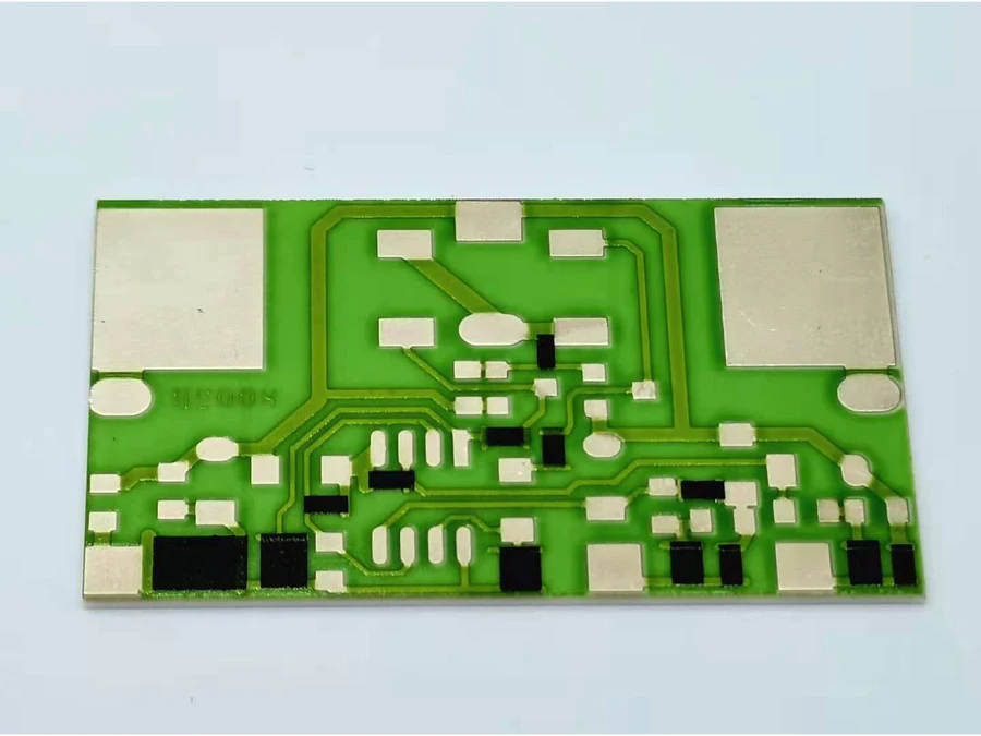
Artwork includes trim allowance, current-path control, measurement points, and final acceptance criteria.
Open product page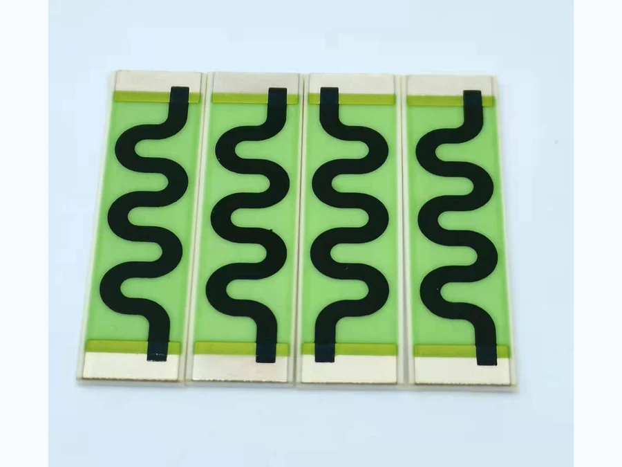
Voltage distribution, geometry, creepage, protection, environment, and test conditions are reviewed together.
Open product pageRFQ checklist
Target resistance or ratio, tolerance, TCR, and reference temperature
Voltage, current, power, pulse, duty cycle, and thermal boundary
Substrate, conductor, termination, overglaze, and assembly route
Available resistor area, trim direction, probe points, and keep-outs
Qualification, sampling, lifetime, and lot-record requirements
Typical programme fit
Suitability and performance are confirmed from the complete assembly and validation conditions, not the application name alone.
Engineering references