
On this page
Prepared by Chipsimple Engineering Team, Engineering and technical content review
Published online August 8, 2026 · Reviewed August 8, 2026
Scope: This guide describes the engineering logic of a conventional fired thick film process. It does not publish a universal print thickness, firing temperature, resistance tolerance, or line-width capability. Those values belong to the selected substrate, paste system, equipment, geometry, and approved process specification.
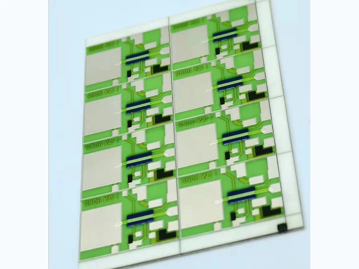
A thick film circuit is not produced by treating each printed layer as an independent graphic. The substrate, conductor, resistor, dielectric, overglaze, terminal finish, and firing sequence form one material system. A change that appears local, such as using a different conductor under a resistor, can change adhesion, contact resistance, trimming behavior, or long-term stability. A credible manufacturing review therefore starts with the complete stack and intended electrical function rather than an isolated picture of the artwork.
Printing controls geometry, but the paste controls how geometry forms
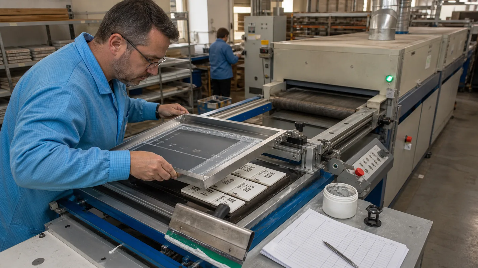
Screen printing transfers a controlled volume of functional paste through patterned openings. The result is affected by screen mesh and emulsion, squeegee condition, print speed and pressure, substrate flatness, paste rheology, environmental conditions, and the time allowed for the deposit to level. These variables are connected. A geometry that prints cleanly with one paste may not behave the same way with another because viscosity, solids content, particle distribution, and recovery differ.
Incoming substrates also matter. Surface contamination can reduce wetting or adhesion. Bow, roughness, chips, and dimensional variation can affect registration or local film thickness. A useful drawing defines the substrate material and grade, finished dimensions, datum scheme, holes or slots, edge restrictions, and any area that must remain free of paste. It should identify which printed features are electrically critical instead of relying only on visual similarity.
Drying and firing are separate process stages
Drying removes volatile components and stabilizes a printed layer before later handling or firing. Firing then removes remaining organics and develops the functional film through a time-temperature-atmosphere profile appropriate to the material system. The peak furnace setting is not the whole specification. Belt speed, zone balance, loading, part orientation, atmosphere, and fixture thermal mass can influence the profile experienced by the workpiece.
The correct profile comes from the material supplier’s data and the manufacturer’s validated process window. A technical data sheet normally identifies a specific paste family, compatible materials, test geometry, processing conditions, and typical properties. Those values should not be copied to another paste or customer design as universal limits. Refiring also requires review because later conductor, dielectric, or overglaze firings can shift an earlier resistor value.
Resistor geometry and laser trimming must be planned together
A printed resistor begins with a target based on sheet resistance and effective squares, but final behavior is not determined by a length-to-width calculation alone. Termination overlap, current crowding, fired thickness, aspect ratio, local heat dissipation, overglaze, and substrate temperature matter. The design also needs trim allowance if laser adjustment is required.
Laser trimming removes a controlled portion of resistive film to increase resistance toward the target. Cut style, location, kerf, remaining current path, measurement method, and stopping rule must fit the geometry. Trimming cannot repair every upstream problem. A resistor that starts outside a sensible as-fired distribution may require an excessive cut, create a hot region, or leave insufficient stability margin. Production control should therefore use an as-fired window and a final acceptance window.
Inspection follows the electrical function
Visual inspection can check continuity, registration, contamination, pinholes, conductor overlap, edge clearance, and trim quality, but appearance alone does not release a functional circuit. Electrical checks may include resistance at a defined reference temperature, continuity, isolation, dielectric withstand, TCR, or a mapped resistance curve. The method depends on whether the printed element acts as a fixed resistor, sensor track, heater, network, or hybrid-circuit element.
For repeat production, the plan should state what is measured, at which stage, with which fixture and instrument, under which conditions, and against which drawing revision. Sampling and lot records are matched to product risk. A prototype report can support release, but it does not replace a controlled batch inspection plan.
Information to provide before process review
- Substrate material, grade, thickness, outline, flatness or bow requirement, and edge restrictions.
- Layer artwork and stack order, including conductors, resistors, dielectrics, protective layers, and terminal finishes.
- Resistance targets, tolerance, TCR or curve requirements, rated load, duty cycle, and reference temperature.
- Assembly operations such as soldering, wire bonding, adhesive attach, coating, or mechanical contact.
- Operating temperature, humidity, fluids, vibration, thermal cycling, and required qualification tests.
- Prototype quantity, expected production volume, drawing revision, and required inspection records.
The practical rule is to approve a material-and-process route, not just a circuit image. When the drawing, functional target, environment, and inspection method agree, printing and laser trimming can be controlled as production processes rather than used as late corrections.
Primary references
- Heraeus Electronics, R 8900 Series Air Fired Resistor System technical data sheet — an example of paste-specific printing, drying, firing, blending, and trimming guidance.
- IEC 60115-1:2020, Fixed resistors for use in electronic equipment — Part 1 — generic terms, inspection procedures, and test methods for fixed resistors.
Need a process review for a real drawing?
Send the layer artwork, substrate, electrical target, assembly method, environment, quantity, and required tests. The route can then be reviewed without assuming unsupported capability values.