
On this page
A current mirror can deliver less current than its reference branch even when the reference resistor is correct. In a basic bipolar mirror, both transistor bases take current from that branch. Before trimming a ceramic bias network, determine whether the missing current belongs to transistor operation, a changing reference voltage or the passive resistor itself. A measured input/output current balance gives the purchasing and analog teams a common way to assign that discrepancy.
System boundary
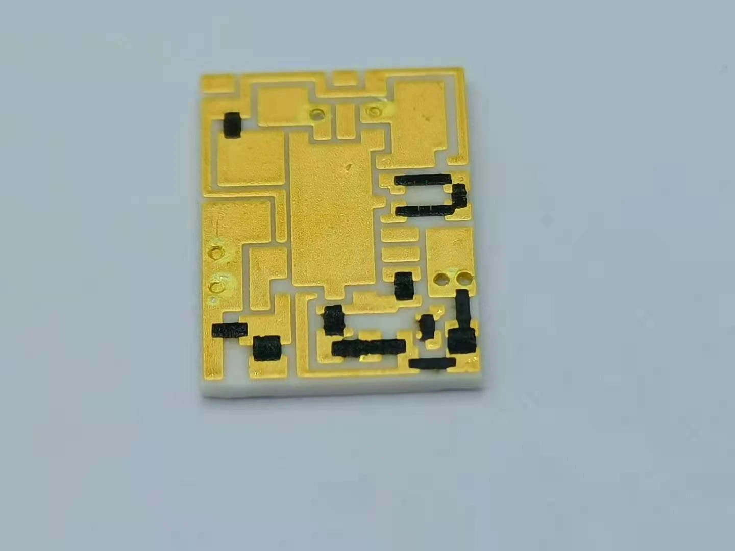
A simple matched two-NPN current sink with common emitters, tied bases and a diode-connected reference transistor. The thick-film circuit supplies passive bias and interconnect functions; semiconductor matching and complete current-source performance require separate validation.
Integration interfaces
| Interface | Required input | Thick film role | Validation owner |
|---|---|---|---|
| Supply and resistor to reference node | Source voltage, resistor and actual reference-node voltage. | Set the drawing-defined passive branch current under the connected voltage. | Analog circuit designer. |
| Reference node to transistor pair | Collector and base-current relationships, matching and temperature. | Provide bias routing without assuming that all resistor current reaches one collector. | Semiconductor integration owner. |
| Mirror output to load | Required output current and allowable output-voltage range. | The passive network cannot guarantee active-region operation of the output transistor. | Load and circuit validation owners. |
Integration risks
| Risk | Control or verification | Validation owner |
|---|---|---|
| Base currents are misclassified as reference-resistor error. | Use the full reference-node current balance. | Analog engineer. |
| One trim at nominal beta is treated as a permanent transistor correction. | Verify across the required operating states and transistor population. | Product validation owner. |
| Output loading drives the mirror outside its valid region. | Check current versus output voltage with the approved low-energy setup. | Circuit owner. |
System integration decisions
- Distinguish current entering the reference node from reference-transistor collector current.
- Calculate finite-beta current loss under explicit matching assumptions.
- Verify current ratio and output-voltage sensitivity separately before trimming.
Draw the reference-current boundary before comparing currents
Consider two NPN transistors with their emitters at the same reference potential and their bases tied together. The first transistor's collector is connected to that base node. A resistor or current source feeds the node, while the second collector provides the output sink. This is the basic two-device mirror, not a Wilson, buffered or MOS mirror.
Name the current entering the shared node Iref. It divides into the first collector and both bases. Calling the first collector current the reference current instead produces a different ratio statement. Preserve terminal directions and measurement locations in the drawing so the circuit calculation and bench report use the same boundary. A passive network tolerance cannot resolve inconsistent definitions.
Include both base-current terms in the input balance
Under the deliberately restricted assumptions of matched transistors, equal collector currents Ic and equal finite current gain beta, each base current is Ic/beta. Current balance gives Iref = Ic plus twice Ic/beta. The output collector current is Ic, so Iout/Iref = beta divided by beta plus two. The ideal unity ratio is approached only when beta is large compared with two.
This calculation ignores unequal collector voltages, mismatch and temperature gradients to isolate one systematic mechanism. In a more general balance, use the individual collector and base currents rather than forcing a common beta. The transistor gain can change with current, temperature and device selection; a single nominal value is not a guaranteed correction factor for every manufactured assembly.
Iref = Ic + 2Ic/beta; Iout/Iref = beta/(beta + 2)
- Iref: total current entering the common collector/base node, in A.
- Ic and Iout: matched collector current and output current, in A.
- beta: equal dimensionless DC collector-current-to-base-current ratio.
Matched two-transistor mirror with equal collector currents apart from reference-node base-current consumption; devices in the intended active region, negligible additional node currents and no Early-effect mismatch.
Calculate how much a nominal-beta trim can actually correct
For an assumed Iref of 1 milliampere and beta of 100, the output is approximately 0.980392 milliampere. Each base draws approximately 9.80392 microamperes. Their sum accounts for the 19.6078 microampere difference. A one-percent resistor tolerance is not the explanation for this roughly 1.96 percent difference in the idealized current balance.
Increasing Iref to 1.02 milliamperes would make the output exactly 1 milliampere at beta equal to 100 in this model. If beta becomes 50 while that adjusted reference current stays fixed, output becomes about 0.980769 milliampere. At beta equal to 200, it becomes about 1.009901 milliamperes. The correction therefore follows the assumed transistor condition, not a universally valid resistance adjustment.
| Assumed beta | Fixed adjusted reference | Calculated output | Interpretation |
|---|---|---|---|
| 50 | 1.02 mA | 0.980769 mA | Base-current loss exceeds the calibrated condition |
| 100 | 1.02 mA | 1.000000 mA | The chosen calibration condition |
| 200 | 1.02 mA | 1.009901 mA | The fixed correction now overcompensates |
Calculate resistor current from its actual voltage
When a resistor Rref feeds the diode-connected node from a supply Vs, its current is (Vs minus Vnode) divided by Rref. The node voltage is not identically zero or a universal constant. For illustrative assumed values Vs equal to 5 volts, Vnode equal to 0.70 volt and Rref equal to 4.3 kilohms, the resistor current is 1 milliampere.
If that same node voltage changes to 0.65 volt with everything else held fixed in the arithmetic example, current becomes approximately 1.011628 milliamperes. This reference-current change is separate from beta-related division. Use the circuit's coupled transistor model or measured node voltage for the actual operating states; do not treat the illustrative node values as a semiconductor temperature coefficient or a universal junction drop.
Keep current-ratio error separate from output compliance
The output transistor must remain in the region where the chosen mirror model applies. Its collector voltage depends on the connected load and supply. Approaching saturation changes the current relationship even if Iref remains stable. A correct reference current and a matched resistor do not prove that the load leaves enough output voltage for the active circuit.
Unequal collector voltages can also change the current ratio through the transistor's finite output resistance before obvious saturation. Sweep or otherwise characterize output voltage within an approved bounded setup while recording both currents. A slope in output current versus voltage is a different signature from a constant base-current deficit. Select the accepted output range from the real circuit, not from a single assumed junction voltage.
Do not confuse emitter degeneration with replacement of base current
Matched emitter resistors can make certain transistor mismatches and output-voltage effects less influential, depending on the complete topology. They also consume voltage headroom. They do not provide the two missing base currents from an external source merely by being present. Reference-node current balance still includes those currents unless another active circuit supplies them.
If emitter resistors are part of the ceramic network, specify their locations, ratio, individual drops and thermal conditions. A design that intentionally uses unequal emitter resistances is not the same unity mirror analyzed above. Likewise, adding a buffer or another transistor changes both current balance and dynamic behavior. Recalculate the actual topology instead of carrying the simple beta-over-beta-plus-two formula into a different circuit.
Measure enough nodes to distinguish the candidate causes
Record the reference resistor voltage and resistance, current entering the common node, output current and output-transistor voltage under the same stable condition. Where direct base-current measurement would disturb the circuit, use a justified model and the observable current balance, retaining its uncertainty. A meter inserted in a branch can add burden voltage and alter the state it is intended to measure.
Compare operating states without changing multiple variables at once. Hold output voltage while investigating reference-source changes, then examine output-voltage sensitivity with the reference state controlled. Keep device temperature and self-heating in the record. A difference that follows transistor population or output voltage calls for an active-circuit review, whereas a measured resistor deviation belongs to the passive network's own acceptance criteria.
Allocate the passive requirement without promising complete mirror accuracy
Provide the full transistor topology, reference-source circuit, load range and intended current definition with the thick-film drawing. Assign resistor tolerance, ratio tracking and dissipation independently from semiconductor beta, matching, leakage and output resistance. If a trim is intended, identify the calibration condition and which residual states must still meet the system requirement.
ChipSimple can review a drawing-defined ceramic bias network and its passive interfaces. The analog designer validates the transistor mirror and any compensation architecture. Keep the base-current budget with the assembly record so a later resistor substitution or semiconductor change does not silently inherit a calibration that was valid only for a different active-device condition.
Review a hybrid current-mirror bias network
Provide the current definitions and active-device boundaries with the resistor drawing.
- Complete mirror and reference-source schematic.
- Required current and output-voltage range.
- Transistor model and current-gain assumptions.
- Resistor voltage, power and matching allocation.
- Calibration condition and retained residual-error tests.
The drawing-upload form loads as you reach this section.