
On this page
A higher alumina percentage is not, by itself, an electrical loss budget. A circuit designer needs to know how much real power the dielectric dissipates at the relevant frequency, voltage and temperature, and whether a proposed material change improves that result in the actual geometry. The useful comparison pairs measured capacitance with dissipation factor under matched conditions. It also separates a material measurement from losses in electrodes, connections and the fixture. This workflow turns a broad request for a higher-purity substrate into a measurable electrical requirement.
Key design decisions
- Define the frequency-dependent loss allocation before changing the ceramic grade.
- Compare capacitance and dissipation factor together, using the same electrical model and operating conditions.
- Resolve fixture and conductor contributions before attributing a small loss difference to alumina.
- Keep dielectric heating, insulation withstand and signal coupling as separate design checks.
1. Define which electric field consumes the loss allocation
Begin with the pair of conductors that establishes the field through the ceramic. A metallized test coupon, a circuit trace over a ground plane and two neighboring conductors do not have interchangeable field distributions. Record the electrode geometry, ceramic thickness, surrounding air gaps and any glass or adhesive in that field. If several materials participate, the measured dissipation belongs to the assembly unless a validated extraction separates them.
Specify whether the allocation concerns continuous heating, resonator performance or another electrical requirement. For a heating allocation, express the permitted real power in watts for the defined region. Do not substitute a limit on coupled current: a capacitor can carry substantial reactive current while dissipating little power. Likewise, an acceptable dissipation result does not establish a safe working voltage or an insulation qualification.
2. Pair capacitance with dissipation factor
For a linear parallel equivalent circuit at one sinusoidal frequency, write the admittance as a conductance G in parallel with a capacitance Cp. The in-phase current produces real power; the quadrature current represents energy storage and return. Dissipation factor D is G divided by the capacitive susceptance. The product of Cp and D therefore matters when two candidates operate at the same frequency and voltage.
Material descriptions may express loss through the imaginary component of permittivity or through loss tangent. A measured loss can include conduction as well as dielectric polarization effects. Retain the definition used in the data rather than combining an intrinsic-material figure with a total assembly capacitance without checking their compatibility.
G = 2πf Cp D; P = V_rms² G = 2πf Cp V_rms² D
- G: parallel conductance in siemens
- f: sinusoidal frequency in hertz
- Cp: parallel-equivalent capacitance in farads
- D: dissipation factor, dimensionless
- V_rms: RMS voltage across the defined conductor pair in volts
- P: real power represented by the parallel loss term in watts
Linear steady-state behavior at the stated frequency and temperature; voltage is across the measured element. Fixture and electrode losses require separate treatment before calling P ceramic loss.
3. Calculate the allowable D from an explicit power limit
Consider an illustrative electrode pair with Cp = 20 pF, operated at 1 MHz and 10 V RMS. Assume D = 0.002 at those conditions. Converting picofarads to farads gives P = 2π × 1,000,000 × 20 × 10⁻¹² × 10² × 0.002 = 0.00002513 W, or approximately 25.13 µW. These are chosen design inputs, not alumina grade specifications.
If the allocation for that same element is 50 µW, rearranging the equation gives Dmax = 50 × 10⁻⁶ / (2π × 10⁶ × 20 × 10⁻¹² × 100), approximately 0.00398. The candidate must still be assessed with measurement uncertainty and relevant operating variation. At 10 MHz, keeping the illustrative Cp and D unchanged would produce 251.3 µW. That calculation demonstrates the frequency multiplier; it does not predict that either material parameter remains constant over the frequency change.
4. Compare complete candidate pairs, not a purity label
Suppose a candidate has half the measured D but a capacitance 20% higher in the same operating geometry. Its predicted power ratio is 1.2 × 0.5 = 0.6, a 40% reduction rather than a 50% reduction. If the ceramic thickness or electrode dimensions also change, record those changes explicitly. Otherwise a geometry-driven benefit may be incorrectly credited to composition.
Use a decision table that keeps the missing input visible. A higher quoted purity can justify requesting relevant characterization, but cannot fill an empty loss field. Price, machining and metallization compatibility remain separate considerations after the electrical comparison.
| Available comparison | Electrical conclusion | Next action |
|---|---|---|
| Same geometry and frequency; Cp and D both measured | Calculate the loss ratio with uncertainty | Check the result against the allocated power across temperature |
| D improves but Cp is unknown | Power improvement is unresolved | Measure Cp under the same conditions |
| Only a low-frequency D value is available | High-frequency loss is unresolved | Use an appropriate measurement method at the application frequencies |
| Purity increases but no electrical data accompany it | No quantified loss benefit established | Request grade-specific frequency and temperature data |
| Assembly loss improves after electrode changes | Benefit belongs to the changed assembly | Separate conductor and dielectric contributions if material selection depends on attribution |
5. Keep the equivalent circuit and fixture consistent
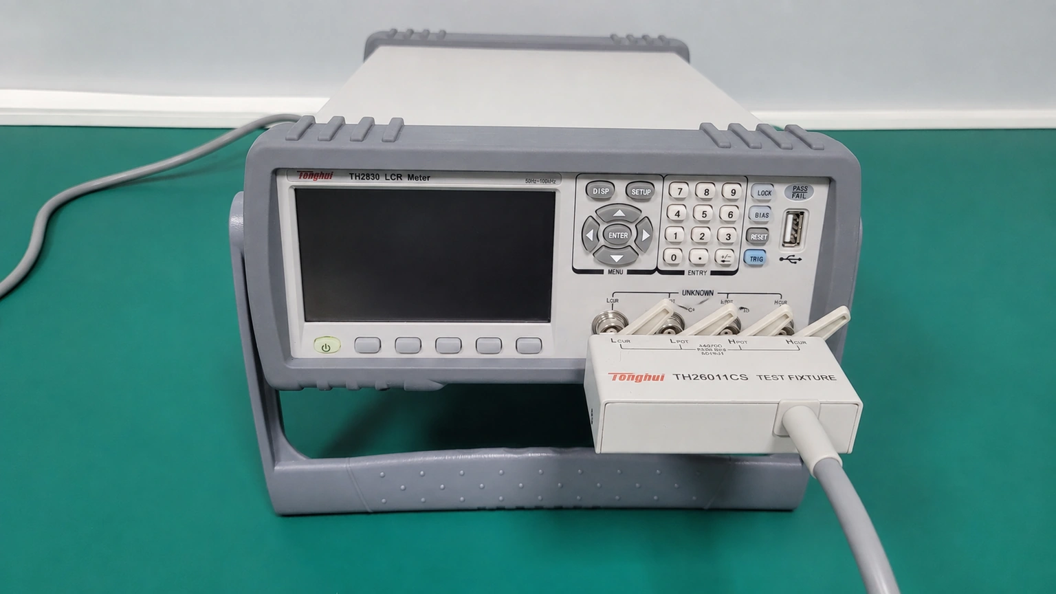
An instrument can report series capacitance with equivalent series resistance, or parallel capacitance with conductance. Record the selected model and the raw impedance or admittance when available. Do not insert a series capacitance into the parallel-power equation merely because both readings use farads. Low-loss approximations may make the capacitances close, but the approximation should be checked against the measured D and the required decision accuracy.
Measure the relevant fixture baseline and establish the compensation procedure at the intended frequency. Connector repeatability, electrode contact and conductor resistance can dominate a very small loss signal. If subtracting the baseline leaves a difference comparable with its variability, report a bounded result instead of inventing additional significant figures. A slightly negative corrected loss is a warning about resolution or correction, not a physically negative dielectric dissipation.
6. Match the frequency and thermal operating envelope
Characterization at one frequency and room temperature is a point, not a complete operating envelope. Choose measurement frequencies around the actual excitation and important spectral components. Materials can be dispersive, and different methods are suited to different frequency ranges. A resonant measurement and a low-frequency impedance measurement must not be compared as though their specimen preparation and uncertainty were identical.
For a nonsinusoidal voltage in a linear system, individual harmonic losses may be summed using each harmonic's RMS voltage and the corresponding frequency-dependent Cp and D. Do not apply the fundamental-frequency D to every harmonic by default. Temperature-dependent data should cover the relevant material temperature, including any heating that the loss budget itself predicts. If the response is nonlinear or temperature is changing appreciably, the simple steady-state calculation needs a more suitable model.
7. Keep low loss separate from insulation and material compatibility
A material can meet a dissipation allocation and still fail an insulation requirement through local field concentration, contamination or a defect. Conversely, an excellent DC insulation result does not supply the missing AC loss tangent. Maintain separate records for dielectric loss, leakage, voltage withstand and environmental durability, with the specimen construction identified in each.
The proposed ceramic also has to work with the metallization, fired glass, resistor system and joining sequence. Do not change substrate composition solely to improve an isolated electrical number while leaving these interfaces unreviewed. Preserve the original geometry for the first electrical comparison where practical, then evaluate any necessary redesign as an additional controlled change.
8. Release a loss budget that another engineer can reproduce
The decision record should contain the geometry revision, material identity, measured Cp and D pairs, instrument model selection, fixture correction, temperature, excitation amplitude and uncertainty. Include the actual formula and unit conversions used to calculate loss. Keep alternative candidates in the same table so that rejected options remain understandable when the operating frequency changes.
Approve a material change against the remaining power margin, not the appearance of a cleaner nominal number. If the margin is smaller than the uncertainty or the operating variation, improve the measurement or revise the allocation before selection. This produces a useful procurement requirement: a defined electrical response under specified conditions, alongside the mechanical and processing requirements for the substrate.
Send the operating conditions for an alumina loss review
Include the electrical field geometry and loss allocation so the material discussion can be tied to the intended circuit.
- Drawing showing electrodes, ceramic thickness and other materials in the electric field
- Operating frequencies or waveform spectrum, RMS voltage and duty cycle
- Material temperature range and allocated dielectric power loss
- Candidate grade identities with matched Cp, D and measurement conditions
- Fixture, compensation, equivalent-circuit model and uncertainty information
- Separate insulation, metallization and joining requirements
The drawing-upload form loads as you reach this section.