
Overview
Thick-film silver paste is a formulated printing material whose metal, glass or inorganic binder, organic vehicle, rheology, substrate interaction, firing history, and downstream assembly determine the fired conductor. The word silver does not identify one universal electrical or joining behavior. Selection must connect the intended current path, pad or trace geometry, substrate, compatible resistor and dielectric layers, firing atmosphere and profile, soldering or bonding route, humidity and contamination, electrochemical potential, protection, inspection, and product validation. Supplier data support candidate screening only for the named material and stated test construction.
Engineering review matrix
Each row links a design variable to evidence that can support a drawing or release decision.
| Variable | Control question | Verification route |
|---|---|---|
| Conductor function | Define electrical net, current, voltage, waveform, allowable drop, pad or trace role, joining/contact route, mechanical load, and accessible potential. | Test resistance, temperature, surface or joint behavior, and insulation in the actual functional geometry. |
| Named paste and revision | Record manufacturer, product code, alloy family, data-sheet revision, lot, storage, conditioning, mixing, screen life, and approved alternatives. | Retain material genealogy and confirm incoming and processed identity under the documented control plan. |
| Printed and fired geometry | Set screen, emulsion, artwork, wet deposit, fired width, gap, thickness observation, edge profile, corners, overlap, pads, and registration. | Measure drawing-linked fired features and correlate them with resistance, continuity, surface, and defect data. |
| Firing and layer sequence | Define drying, atmosphere, furnace profile, loading, print/fire order, refires, compatible resistor/dielectric/protection layers, and downstream heat. | Record actual process history and compare electrical, adhesion, surface, and interface results after every material stage. |
| Assembly interface | Specify finish, solder alloy/flux, adhesive, wire or spring contact, profile or cure, cleaning, pressure, rework, strain relief, and inspection. | Qualify the exact pad and joint/contact system with electrical, physical, and relevant mechanical/environmental evidence. |
| Environment and bias | Define temperature, humidity, condensation, contaminants, fluids, voltage gradient, polarity, current, duty, storage, cleaning residues, and protection. | Run configuration-specific biased and unbiased exposures and inspect leakage, migration, corrosion, resistance, and physical change. |
| Acceptance and change | Set dimensional, electrical, surface, adhesion or joint, insulation, sampling, records, substitutions, supplier change, process change, and requalification rules. | Use traceable product/coupon correlation and repeat affected tests before accepting a material or process change. |
Controlled model
Fired conductor resistance and selection comparison
Translate a circuit need into a fired conductor requirement, then treat wet printing and firing as transformations whose outputs must be measured. Ideal resistivity equations cannot represent porosity, thickness profile, glass phase, surface, conductor-resistor interaction, corners, pads, or joints without correlation.
R = ρ L/(W t)First-order resistance of a uniform rectangular fired conductor.
- Units
- R in Ω; ρ in Ω·m; L, W, t in m
- Use boundary
- Uses effective fired geometry and resistivity. It omits porosity, edge profile, corners, interfaces, contact resistance, current crowding, and temperature dependence.
P_loss = I²R_pathScreens conductor-path electrical heating at a defined current.
- Units
- W
- Use boundary
- Does not predict local temperature without current distribution, substrate, neighboring heater or resistor heat, interfaces, and duty.
Decision comparison
| Decision | Route A | Route B | Verification |
|---|---|---|---|
| Pure-silver-rich versus silver-alloy conductor family | A silver-rich route may offer one balance of fired conductivity and processing, but migration, solder interaction, adhesion, cost, and compatibility remain system-specific. | Silver-palladium or another alloy family may change solderability, leach behavior, resistance, firing, bonding, and cost; the alloy name alone does not rank reliability. | Compare named data sheets and production-intent samples using the same substrate, geometry, layers, firing, assembly, bias, environment, and acceptance plan. |
| Trace conductor versus assembly pad | A routing trace prioritizes controlled resistance, print definition, current distribution, layer interaction, and spacing. | A solder, adhesive, spring-contact, or wire-bond pad adds surface, finish, joint, dissolution, force, cleaning, and rework requirements. | Validate each function with its actual geometry and downstream process; do not qualify a pad from a simple fired-line coupon. |
- Paste storage, conditioning, mixing, screen life, print pauses, drying, firing, and refires can change output and require controlled supplier instructions.
- A supplier firing temperature is a material-process condition, never a finished circuit operating-temperature claim.
Failure controls
These are review prompts, not evidence that every risk applies or that every test is available.
- A
Selecting by the word silver or by nominal conductivity while ignoring alloy, glass system, substrate, firing, geometry, layers, and joining.
- B
Transferring supplier coupon typical values to a different print thickness, refire history, conductor length, pad, environment, or finished product.
- C
Using one paste for traces and assembly pads without verifying solder dissolution, wire bonding, adhesive, spring contact, cleaning, and rework needs.
- D
Ignoring humidity, residues, spacing, potential difference, protection defects, and polarity in electrochemical migration or leakage risk.
- E
Changing firing profile, layer order, resistor, dielectric, overglaze, substrate, finish, joint, or cleaning after approval without requalification.
- F
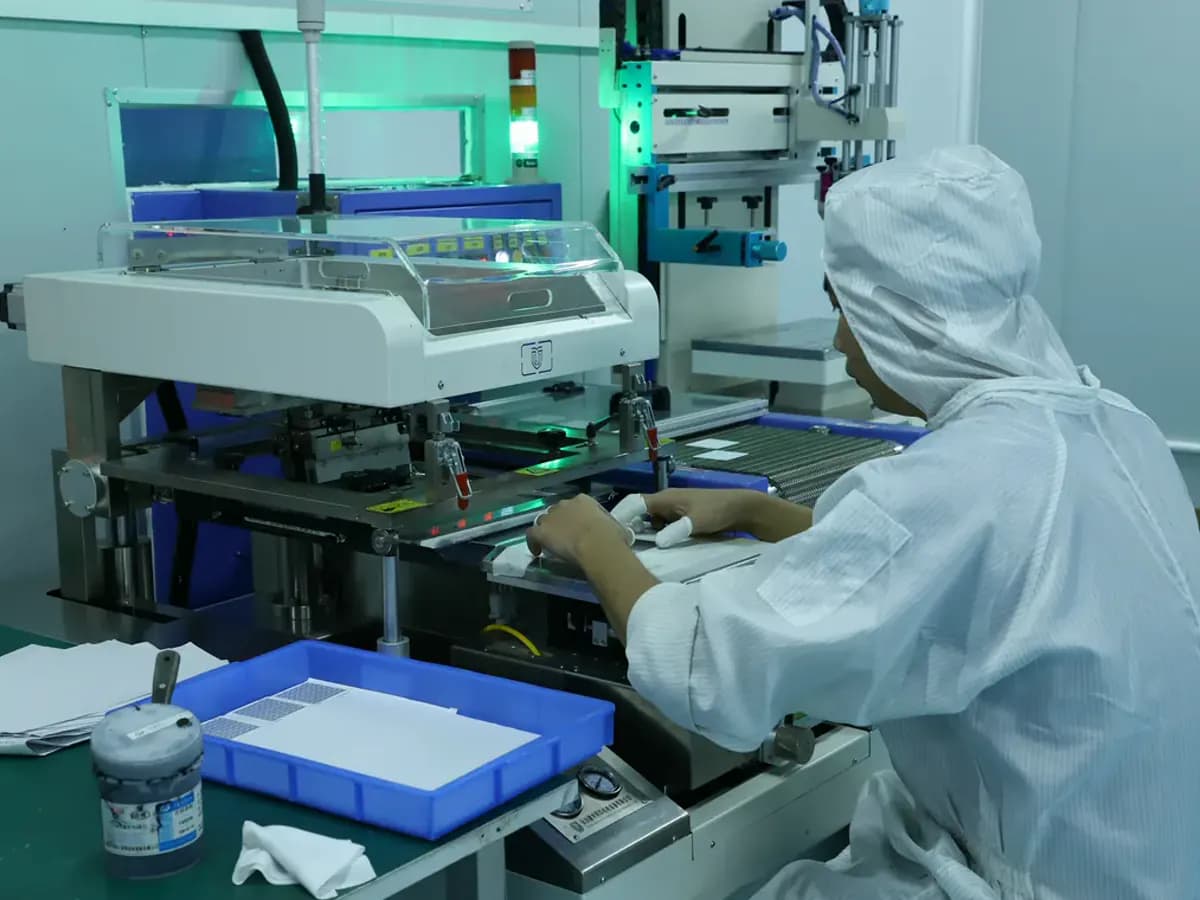
Turning a printing-equipment or product photograph into evidence of paste identity, capability, adhesion, conductivity, migration resistance, or qualification.
Silver-conductor selection workflow
The order makes assumptions and ownership visible before a result is promoted to a requirement.
- 01
Define conductor functions
Separate routing traces, crossovers, via interfaces, resistor terminations, solder pads, wire-bond pads, adhesive pads, spring contacts, shields, and heaters. For each, state resistance, current, voltage, spacing, surface, joining, mechanical, environment, and inspection needs.
- 02
Build the compatibility matrix
List substrate, conductor code, resistor, dielectric, overglaze, firing and refire order, atmosphere, finish, joint materials, flux or adhesive, cleaning, protection, and assembly heat. Record which combinations are supported, conditional, unknown, or evidence needed.
- 03
Design printable geometry
Set finished trace width, gap, pads, overlaps, corners, vias, registration, edge distance, screen, emulsion, wet and fired thickness observations, and inspection datums. Evaluate conductor resistance and local current paths at dimensional and material tolerances.
- 04
Control printing and firing
Follow the named supplier's storage, conditioning, mixing and processing instructions, then define printing, leveling, drying, firing, atmosphere, belt loading, refires, handling, and traceability. Do not invent a universal profile or accept visual appearance as sufficient control.
- 05
Validate interfaces and environment
Measure geometry, resistance and continuity; inspect adhesion and surface; execute the specified solder, bond, adhesive or contact route; and test humidity/bias, contamination, cycling, current, corrosion, or other owned conditions on representative construction.
- 06
Freeze material and changes
Tie approval to supplier/product code and revision, lot controls, complete stack, artwork, print/fire window, downstream assembly, inspection, sampling, environment, and requalification triggers. Any capability statement must remain limited to the evidence available for the named configuration and responsible technical review.
Reference boundary
Public method sources
These sources support the engineering method and terminology used in this technical guide. They do not establish a ThickFilmPCB material list, capability limit, customer result, certification, or finished-product specification.
- 01Heraeus — C2130B silver/palladium conductor technical data sheet
Supports linking one named conductor to substrate, printing, firing, fired thickness, resistance, adhesion, solder and leach test context. Its values are supplier-specific and not ChipSimple evidence.
- 02DuPont LF181 conductor technical data sheet
Supports reviewing one named conductor's stated processing, fired properties, adhesion and assembly context only. It does not establish interchangeability or any company production result.
- 03IPC J-STD-003D — Solderability tests for printed boards
Supports solderability and resistance-to-dissolution method boundaries within its scope; it does not select a thick-film silver paste or qualify a ceramic product joint.
Inputs for a practical review
Unknown values may be labelled unknown. The review should convert uncertainty into an explicit decision or validation task.
Send Drawings- 01
Circuit artwork and net table with trace/pad functions, current, voltage, allowable drop, spacing, waveform, grounding, and accessible metal.
- 02
Substrate and full printed material stack, required or prohibited paste families, firing sequence, refires, protection, and substitutions.
- 03
Finished trace, gap, pad, overlap, via, edge, hole, registration, thickness, flatness, and critical inspection dimensions.
- 04
Solder, wire bond, conductive adhesive, spring contact or other interface; finish, heat/cure, flux, cleaning, force, rework, and strain relief.
- 05
Temperature, humidity, condensation, contaminants, fluids, bias, polarity, current, cycling, storage, and corrosion or migration criteria.
- 06
Resistance, continuity, adhesion, solderability/bond/contact, leakage, withstand, environment, inspection, sampling, and acceptance methods.
- 07
Prototype alternatives, quantities, traceability, supplier/data-sheet revision, reports, drawing revision, and change-control triggers.