
On this page
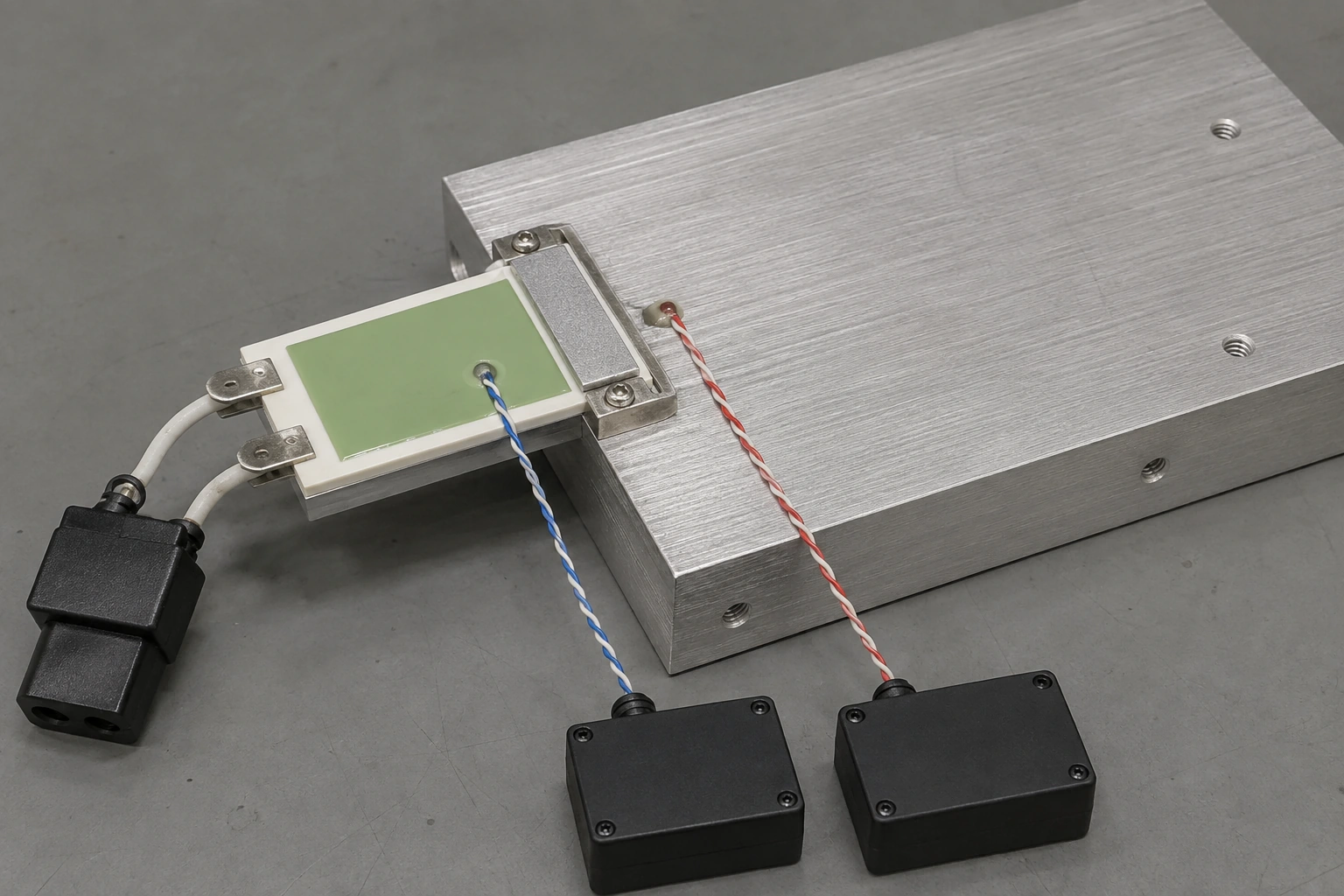
A ceramic circuit placed beside a fast power switch occupies electrical, thermal and mechanical fields simultaneously. Gate or sensing conductors can couple to a switch node; insulation distances depend on the complete assembly; heat-sink attachment can bend ceramic or create a conductive path; local heating changes resistor behavior. The interface must identify potentials, current loops, thermal contacts, substrate supports and measurement reference. ChipSimple can review drawing-defined thick-film features. Semiconductor limits, insulation coordination, control safety and module qualification remain customer responsibilities.
System boundary
The boundary includes power semiconductor terminals, switching loop, auxiliary ceramic circuit, gate or measurement paths, substrate, overglaze where specified, interconnects, insulation system, heat spreader or sink, supports, enclosure and controller. ChipSimple review is bounded to the supplied circuit drawing and application inputs.
System integration decisions
- Map normal and transient potential for every conductor and nearby metal.
- Define sensitive return loops before routing around the switch node.
- Separate heat removal from ceramic mechanical support.
- Validate parasitic coupling in the installed stack rather than bare card alone.
Create an assembly-level potential map
Label semiconductor nodes, printed conductors, guards, sink, fasteners, shields and controller references under normal switching and defined faults. Include common-mode movement, not only DC voltage. A metal support that is safe at one potential can alter clearances when floating. The map must use actual assembly coordinates and material boundaries. It becomes an input to qualified insulation work; it is not itself a voltage rating.
Draw switching and sensitive current loops
Trace commutation current, gate drive, current sensing, temperature sensing and auxiliary supply returns. Shared conductor or inductance can turn power current change into signal voltage. Keep the physical return beside its forward path where the design requires field cancellation. Record interconnect length and connection order. A schematic net label does not show loop area or where a current actually returns through a plane, sink or cable.
Screen capacitive injection from a switch node
A first estimate relates parasitic capacitance and voltage slew to displacement current.
i_c=C_p(dv/dt); V_err≈i_c Z_in
- C_p is effective capacitance from switch node to the sensitive node.
- dv/dt is the relevant voltage transition rate.
- Z_in is the frequency-dependent receiving impedance.
Linear small parasitic and simplified impedance; distributed fields, nonlinear protection and common-mode conversion require measurement or electromagnetic analysis.
Calculate an illustrative coupling event
For an assumed 2 pF coupling and 8 kV/µs transition, displacement current is 16 mA during the edge. If the relevant high-frequency impedance were 12 Ω, the simple estimate gives 0.192 V. These values are not module or card capabilities. They show why tiny capacitance can matter during fast switching and why bandwidth and physical layout belong in the interface.
Keep printed geometry inside the complete insulation design
Working voltage, transients, pollution, altitude, material group, coating, temperature and aging influence creepage and clearance decisions. Overglaze is not automatically a certified barrier. Interfaces, edges, holes and contamination can dominate. The customer safety authority selects requirements and validates the assembly. ChipSimple can hold reviewed artwork distances by drawing but cannot infer an isolation rating from a photograph or generic ceramic property.
Map heat-generating locations and sensor references
List semiconductor loss, resistor dissipation, gate-driver loss and external sink boundary. Determine which ceramic elements experience local gradients. A sensor on the sink may not represent a resistor near a switch. Use measured or reviewed properties without importing competitor values. Evaluate transient and steady states because the thermal mass and control duty can produce different peaks.
Support ceramic without creating an uncontrolled heat or force path
Define flatness, compliant interface, preload, support points, adhesive, fastener sequence and expansion mismatch. A thermal interface may require pressure while brittle ceramic requires controlled bending. Holes and edges need drawing-specific review. Cable or busbar loads should react through structure rather than terminals. Verify the assembled contact and strain over temperature and vibration states specified by the integrator.
Assign evidence for each coupled domain
The allocation prevents one successful electrical test from approving every boundary.
| Domain | Required record | Owner |
|---|---|---|
| Switching field | Waveforms and physical loop geometry | Power-electronics owner |
| Signal integrity | Raw error versus switching state | Control-circuit owner |
| Insulation | Potential map, materials and qualified assessment | Safety authority |
| Thermal | Loss map and local temperatures | Thermal owner |
| Mechanical | Support, preload, flatness and strain | Mechanical owner |
Measure without changing the phenomenon
Probe capacitance, ground leads and isolation equipment can create new current paths. Document probe model, bandwidth, connection location and cable route under the customer test procedure. Compare power-stage disabled baseline with controlled switching states. Capture switch node, sensitive node and reference simultaneously. Do not use an unsafe floating instrument or defeat protective barriers for cleaner data.
Validate the installed module across coupled states
Inspect the ceramic circuit and mounting first. Exercise representative voltage transitions, current, thermal states and control modes within qualified limits. Record signal error, switching waveform, local temperatures and mechanical condition. Apply only customer-approved faults. The integrator owns semiconductor stress, insulation, control response and product safety. ChipSimple review remains limited to drawing-defined passive circuit features.
During switching evaluation, correlate the switch-node waveform with the voltage observed at the measurement reference and with temperature at the local dissipating features. The acquisition plan should state probe loop area, attenuation, bandwidth, common-mode limit and timestamp alignment. Repeat the capture after changing only one coupling path, such as gate resistance, conductor spacing or shield termination. If the apparent disturbance follows the probe arrangement rather than the hardware change, treat it as a measurement artifact. If it follows switching edge rate while the reference remains controlled, investigate capacitive or inductive injection. This disciplined comparison prevents an oscilloscope image from being promoted into an isolation or reliability conclusion.
Reopen review when geometry or switching changes
Changes to semiconductor, switching speed, gate drive, busbar, cable, sink, barrier, support, interface, artwork, receiver or enclosure alter coupling. A firmware change to edge rate can invalidate signal evidence while the card is unchanged. Bind electrical waveforms and assembly revisions to each result. Reassess affected electrical, thermal and mechanical domains rather than recalibrating one output.
Do not imply module ratings from a ceramic circuit page
This page establishes an interface method, not voltage, power, isolation, temperature or lifetime capability. Numerical values are illustrative. Actual construction and tolerances remain by drawing and application review. If the potential map, switching waveform or mechanical stack is missing, the integration decision remains open.
Provide the complete power-module field and stack
Circuit review needs electrical potentials, loops, losses and mechanical support.
- Power topology, switch-node waveforms, fault states and control references.
- Ceramic circuit drawing, passive network, terminals and sensitive nodes.
- Insulation requirements, barriers, environment and safety ownership.
- Loss map, cooling, sink, interface and temperature states.
- Support, preload, interconnects, vibration and validation method.
The drawing-upload form loads as you reach this section.