
On this page
An alumina purchase description must tell receiving inspection and printing which physical face and reference features matter. A material grade and outline drawing alone do not establish whether the supplied surface, free-state shape or edge references are suitable for the intended conductor-and-resistor pattern. This guide shows how to turn those downstream needs into an incoming-substrate specification and a matched print trial without inventing a universal flatness or fine-line capability.
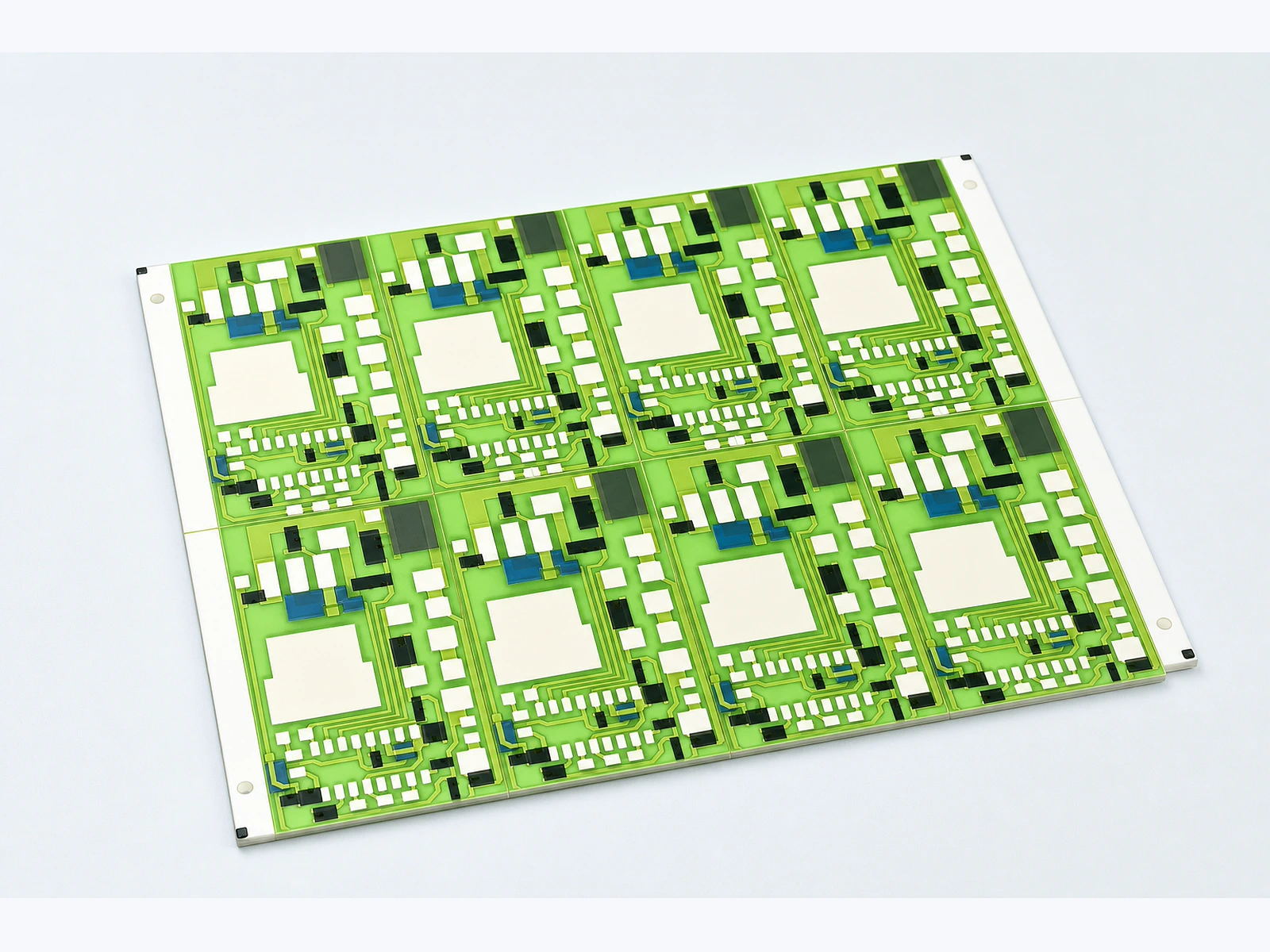
For a drawing-specific part, review the Alumina thick film PCB construction, product evidence and quotation inputs alongside this method. Prepare the dfm checklist with your operating conditions.
Key design decisions
- Name the print face and its supplied surface state instead of relying on the material grade to imply them.
- Separate free-state substrate geometry from the shape created by vacuum, clamps or a printing nest.
- Reference fired-feature position to functional ceramic datums that remain available at inspection.
- Approve the purchase description from traceable incoming maps and matched print evidence, not from an isolated best coupon.
1. The purchase form is a process input
A substrate lot can meet its nominal material description and still arrive in a form that creates avoidable ambiguity at printing. The two faces may have different histories, an edge may have been selected as the manufacturing reference, or a surface treatment may be stated only on packaging. If the drawing does not identify the face and datum used by the artwork, receiving inspection cannot confirm that production is starting from the intended condition.
Write the purchase requirement around observable attributes: material designation, thickness, outline revision, identified print face, supplied surface description, edge condition, datum features and the state in which shape is measured. Values remain drawing-specific. This page does not publish a company purity range, flatness limit, roughness limit or printable feature size. Those items require controlled product and process evidence for the actual project.
2. Identify the print face and preserve its datum chain
Use an asymmetric feature, controlled mark, packaging orientation or other agreed method to distinguish the print face when the outline itself is symmetric. The identification method must survive receiving, cleaning and placement without contaminating the functional surface. A note such as “polished side up” is inadequate if the receiving method cannot distinguish that side consistently or if polishing has not been confirmed for the supplied grade.
The artwork origin should trace to ceramic features that can be measured after firing. An outline corner may be convenient, but chipped edges, edge finishing or loose fixture contact can move the effective reference. Holes, slots or dedicated fiducials may form a better datum scheme when the drawing and inspection access support them. Record the precedence of primary, secondary and tertiary references so that a different operator cannot silently reverse the coordinate convention.
3. Measure free-state shape before the nest changes it
Flatness data are meaningful only with a stated support condition. Map the ceramic in a defined free or minimally supported state before vacuum or clamps force it against a printing nest. A restrained reading describes the combined part-and-fixture condition; it must not replace the incoming free-state record. Use the same face orientation, support points, temperature and coordinate grid when comparing lots.
Retain the signed height map rather than only its peak-to-valley value. Two substrates can have the same range while one has a smooth bow and the other has a local high region beneath a critical print. Flip-and-repeat measurements can expose support bias or face-label errors, although they do not automatically separate every measurement artifact. Report instrument resolution, repeat setup behavior and any filtering applied to the surface data.
4. Keep surface state separate from alumina grade
As-fired, lapped and polished surfaces describe processing states, not interchangeable quality levels. A smoother surface may change print definition or contact with the screen, yet it can also change cleaning, handling and paste-interface behavior. Selection therefore belongs to the complete substrate-and-paste route. Do not transfer a surface requirement from a thin-film, bonding or optical application merely because the same alumina designation appears in both projects.
Record incoming observations that can be reproduced: the named face, visible damage or residue, the controlled surface document supplied with the lot, and any agreed measurement. Avoid turning an unverified appearance into a roughness value. If adhesion, fired geometry or resistor behavior depends on the surface state, resolve that relationship with a matched process trial using the intended paste system and firing sequence.
5. Run a matched conductor-and-resistor print trial
Divide traceable substrates from each candidate incoming condition across a trial that holds artwork, screen, paste lot, printing settings, drying, firing profile and measurement method constant. Randomize or interleave the groups where time-dependent paste or equipment drift could bias the result. The purpose is not to crown a generally superior alumina surface; it is to determine whether the proposed purchase description controls the features important to this circuit.
Inspect conductor edges, registration to ceramic datums and the fired state relevant to subsequent resistor printing. Then evaluate resistor geometry and electrical observations under their stated test conditions. Preserve individual results and panel or carrier positions. An acceptable group average can conceal a position-dependent registration error, while one poor coupon cannot establish a substrate cause without comparison evidence.
6. Calculate registration from the measured datum
For one coordinate axis, define the fired feature position relative to its measured ceramic datum as x_feature - x_datum. Compare that relative position with the artwork offset x_artwork: e_reg = (x_feature - x_datum) - x_artwork. All three coordinates must use the same sign convention, units and measurement temperature. The residual is a location error for that feature; it is not a substrate flatness measurement.
Suppose x_feature is 25.060 mm, x_datum is 0.020 mm and x_artwork is 25.000 mm. The residual is +0.040 mm in the declared positive direction. Repeat the calculation for distributed features in both axes. A single number cannot distinguish translation, rotation, scale and local distortion, so fit only the global terms supported by the datum set and reserve independent features to check the remaining residual.
| Item | Example value | Interpretation |
|---|---|---|
| Measured feature coordinate, x_feature | 25.060 mm | Coordinate in the declared inspection axis |
| Measured datum coordinate, x_datum | 0.020 mm | Observed datum position in the same setup |
| Artwork offset, x_artwork | 25.000 mm | Nominal feature position relative to that datum |
| Registration residual, e_reg | +0.040 mm | Signed deviation; drawing acceptance remains project-specific |
7. Read the residual pattern before changing the substrate
A nearly constant x-y shift across every substrate suggests an artwork origin, fixture location or datum-transfer issue. Residual that changes approximately with distance from the origin suggests scale or thermal-coordinate mismatch. Opposite-signed errors across the field are more consistent with rotation. A local cluster near a support point can implicate seating or shape, but the support condition must be changed deliberately before that mechanism is assigned.
If only one named face produces poor definition, verify face identity, cleaning and the documented supplied surface state. If edge quality changes while registration remains stable, investigate screen, paste, drying and firing variables rather than forcing the explanation into substrate flatness. Each corrective trial should change one discriminating boundary and retain an unchanged control. Report unresolved alternatives when the data do not separate them.
8. Release a specification that both teams can audit
The final purchase description should identify the controlled substrate document, print-face convention, free-state measurement support, datum scheme, inspection grid and required records. Link the matched print trial to the represented substrate group and circuit revision. If a later source, surface process, thickness, edge process or datum changes, reopen only the affected evidence rather than assuming the previous result transfers unchanged.
For an engineering quotation, send the substrate drawing together with the mixed conductor-and-resistor artwork and the downstream measurement plan. State which requirements are fixed, which are proposed for trial and who owns acceptance. This allows the substrate supplier, printing process and customer validation team to discuss the same physical references without converting an early material-selection study into an unsupported manufacturing promise.
Send the alumina substrate and print-datum package
Provide enough information to connect the supplied ceramic condition to the mixed conductor-and-resistor printing task.
- Current substrate drawing, material designation, thickness and outline revision
- Print-face identification method and controlled description of the supplied surface state
- Primary, secondary and tertiary ceramic datums with artwork origin and axis convention
- Free-state shape or flatness measurement support, grid, temperature and required record format
- Conductor and resistor artwork, paste-system constraints, drying/firing sequence and critical feature locations
- Matched-trial quantities, inspection method, electrical test conditions and project acceptance owner
The drawing-upload form loads as you reach this section.