
On this page
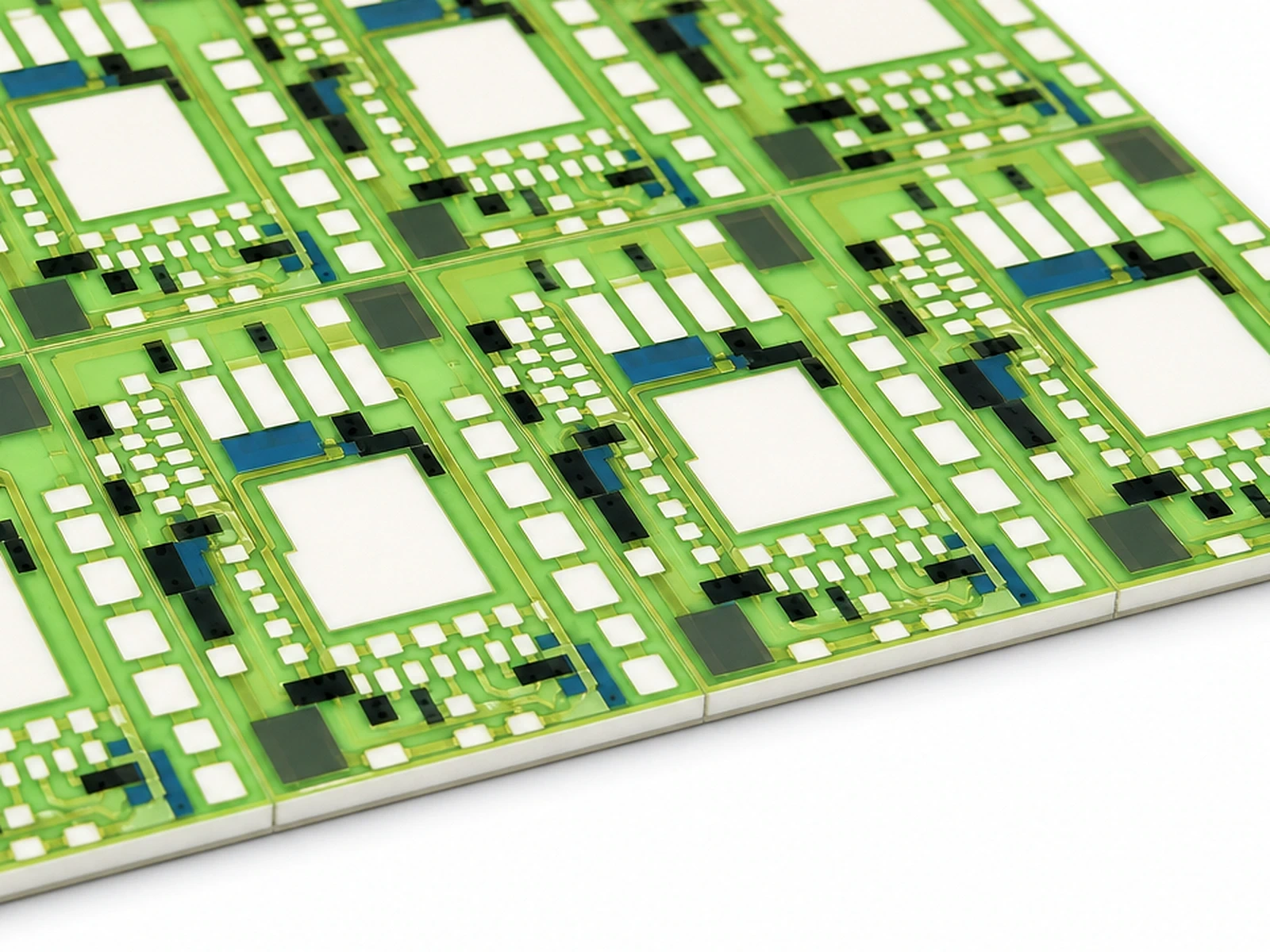
Fired overglaze protects selected thick film regions while leaving connection pads, contact tracks and adjustment areas accessible. Its artwork therefore defines a functional boundary, not merely a colored finish. A clear green surface should correspond to controlled coverage, thickness and openings on the actual circuit. Specify where protection is required and where glass must not intrude, then evaluate the finished boundary after firing and all relevant assembly steps.
Key design decisions
- Separate the protected circuit region from soldering, bonding, probing and active wiper-contact windows.
- Allocate opening margins to printed-edge variation, registration and the actual contact footprint.
- Judge coverage and edge definition on the fired layer, with the material grade and complete thermal sequence recorded.
Map the functions that need protection or access
Identify the conductors and resistors to be covered, the pads that must remain exposed and any active contact path that cannot tolerate glass intrusion. A sensor wiper track and a solder pad have different access requirements, even if both appear as openings in the overglaze artwork. Mark their functions explicitly.
Distinguish a protective overglaze from the primary dielectric insulation beneath a crossing or heater. The layers may have different jobs and material requirements. A visually attractive glass surface does not automatically establish a required insulation barrier, chemical resistance or hermetic enclosure. Those functions need their own material and assembly evidence.
Specify the material state behind the green finish
Green overglaze appearance is a property of a particular formulation and fired state. Color does not establish film thickness, density or suitability for another circuit. Compare the processed layer under consistent lighting while retaining the separate dimensional and electrical checks required for its protective function.
For a product drawing, record the actual overglaze grade and the required finished condition. If visual consistency matters, use controlled illumination and an approved physical appearance range from real parts. Avoid asking an image to imply a thicker or more complete glass layer than the product has. Functional coverage and the real surface state take precedence over a cosmetic rendering.
Calculate the usable opening at its limits
Begin with the footprint of the operation that needs access: solder wetting, a bond tool, a test probe or a moving contact. Add the positional variation of that operation, then compare it with the smallest finished overglaze opening. The nominal exposed metal area can overstate usable access if the glass boundary moves toward the contact.
Include registration between the overglaze and underlying conductor, printed-edge variation and any assembly placement allowance. Evaluate the directions separately when the contact footprint is elongated. A generous opening in one direction cannot compensate for glass encroachment across the narrow dimension.
Wusable,min = Wopening,nom − 2Eedge − 2Erelative
- Wusable,min: conservative minimum accessible width
- Wopening,nom: nominal opening width in the evaluated direction
- Eedge: inward boundary allowance per side
- Erelative: relative displacement allowance used for a centered contact envelope
A symmetric geometric screening model. Asymmetric registration and contact footprints should be checked with explicit boundary overlays rather than forced into this expression.
Inspect the boundary where it changes circuit function
A boundary should be evaluated for position, continuity and local shape. Small waviness far from a functional feature is different from a protrusion into a solder window or a void exposing a vulnerable trace. Define the critical regions on the drawing so inspection attention follows function.
Inspect the fired boundary under lighting that distinguishes translucent glass from the underlying metal and ceramic. A strong reflection can make a sound edge appear irregular, while a dark image can hide thin coverage. Use consistent views for comparisons and retain the original photograph before any presentation cleanup.
Compare the opening boundary with the assembled contact footprint using a common datum. Inspecting the glass and conductor independently can miss a relative-position error even when each individual outline appears acceptable. Retain that overlay for the most constrained pad or moving-contact region, where a small inward shift has the greatest functional consequence.
Use opening rules specific to the next operation
The same opening size should not be copied across unrelated interfaces. The material must remain accessible in the way it will actually be used, including tool approach and motion.
| Exposed region | Access requirement | Defect to exclude |
|---|---|---|
| Solder pad | Wettable area and fillet envelope | Glass intrusion that reduces the joint area |
| Wire-bond pad | Landing footprint and tool clearance | Glass near the bond footprint or tool edge |
| Electrical test pad | Repeatable probe contact | Probe landing partly on glass |
| Wiper-contact track | Continuous active travel path | Raised glass within the moving-contact region |
| Trim region | Defined adjustment access | Coverage incompatible with the selected trim sequence |
| Connector contact | Installed contact overlap | Opening too small at mating and registration limits |
Coordinate overglaze with trimming and assembly
The order of resistor trimming, glass firing and later attachment affects which surfaces are accessible and which thermal exposures the resistor sees. Define the intended sequence with the selected material system. Do not assume every overglaze can be applied before or after every trim process.
Measure relevant electrical values before and after the glass operation under matched temperature and contact conditions. A resistance change can result from the added thermal exposure or material interaction rather than from an apparent change in visible resistor geometry. Keep an appropriate comparison condition if the cause matters to the design.
Avoid confusing average thickness with complete protection
A thickness measurement on a broad flat region does not establish coverage over a conductor step or beside a narrow opening. Select measurement locations that represent the difficult geometry. If a defect is suspected, examine the local region rather than increasing every layer indiscriminately.
More material can change leveling, opening size and thermal history. The appropriate correction may be a revised boundary, improved surface preparation or a controlled print sequence rather than a thicker nominal coating. Use the selected overglaze's processing guidance and verify the actual circuit geometry.
Deliver coverage artwork with functional acceptance points
Provide a protection map, named opening regions, underlying conductor artwork and the final-state inspection requirements. Identify which boundaries are cosmetic and which directly control electrical or assembly function. Include the intended firing and assembly sequence so the receiving team knows when the opening must be verified.
For a circuit review, add the relevant solder, bond, probe or contact footprint and its placement allowance. This makes the discussion about a measurable usable region rather than a vague request for a clean-looking green coating. The finished product should show its real, sharply defined glass coverage without hiding the interfaces that the customer needs to use.
Submit the overglaze coverage package
Provide the protected regions and the access requirements of every opening.
- Overglaze and conductor artwork with solder, bond, probe, trim and moving-contact regions identified.
- Material grade, layer sequence, fired thickness information and final surface appearance requirements.
- Contact or tool footprints, placement allowances and critical boundary dimensions.
- Fired-boundary photographs, electrical changes across processing and any local coverage concerns.
The drawing-upload form loads as you reach this section.