
On this page
A resistor ratio used to set amplifier gain can also determine the damping of an active low-pass filter. Adjusting that ratio until the low-frequency output is correct may therefore leave the frequency response outside its intended envelope. For a printed network supplied into a Sallen-Key stage, the drawing and electrical specification should identify the gain-setting elements, timing elements and external capacitors as separate functional groups.
Key design decisions
- Specify pole frequency and damping separately from the low-frequency gain.
- Translate the allowed damping window into a permitted gain-resistor ratio, rather than assuming the gain tolerance is sufficient.
- Test the assembled frequency response where capacitor, amplifier and connection effects are included.
Identify which resistors set timing and which set gain
Define R1 from the signal input to an intermediate node and R2 from that node to the amplifier's noninverting input. Place C1 from the noninverting input to the small-signal reference and C2 from the intermediate node to the amplifier output. The amplifier's separate negative-feedback pair sets noninverting gain K = 1 + Rf/Rg. These labels fix the topology used in the following equations.
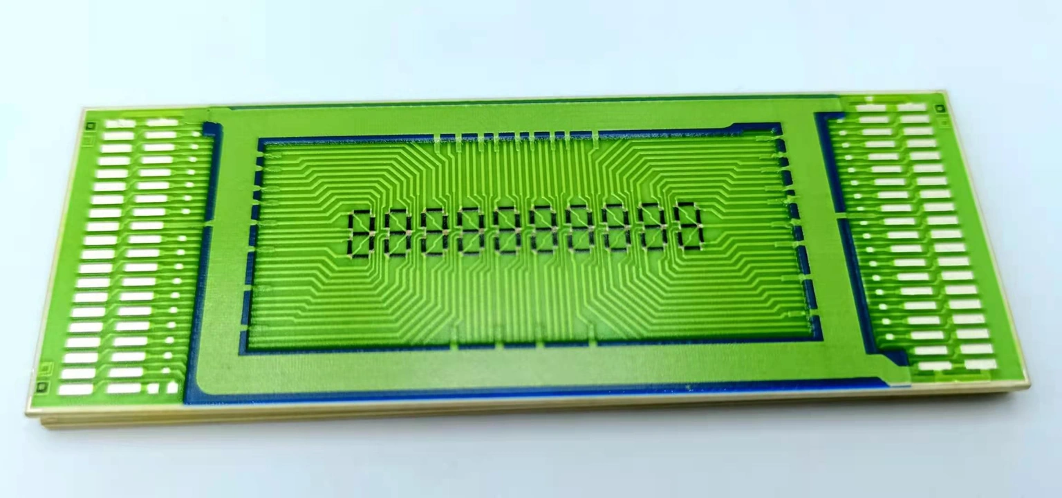
A ceramic thick-film network may contain the two timing resistors, the feedback pair or all four. The external capacitors and active amplifier still determine the assembled response. State the supply boundary and the actual network terminals. Do not describe a passive printed resistor array as a complete filter when the active and capacitive elements are supplied elsewhere.
Keep gain, pole frequency and damping as three requirements
For ideal equal timing resistors R1 = R2 = R and equal capacitors C1 = C2 = C, the transfer denominator is (sRC) squared plus (3 minus K)sRC plus one. The natural pole frequency is f0 = 1/(2 pi RC), and the quality factor is Q = 1/(3 minus K). The low-frequency signal gain is K. Thus RC sets the frequency scale, while the gain pair also controls damping.
The pole frequency is not automatically the frequency at which amplitude is three decibels below the passband. That equality occurs only for the appropriate damping. A drawing that states only cutoff frequency can therefore hide different interpretations. Name the frequency definition, the allowed response shape and whether gain is normalized to the measured passband or expressed as an absolute voltage ratio.
H(s) = K / [(sRC)^2 + (3 - K)sRC + 1]; f0 = 1/(2 pi RC); Q = 1/(3 - K)
- K = 1 + Rf/Rg is the ideal noninverting passband gain.
- R is each equal timing resistance in ohms; C is each equal timing capacitance in farads.
- s is complex frequency in inverse seconds; Q is dimensionless.
The stated topology has equal timing components, negligible source loading and an amplifier behaving ideally over the evaluated band. These formulas do not characterize the complete high-frequency stopband.
Convert a damping limit into a gain-ratio window
Assume a stage requires K = 2.5 and Q = 2. The nominal feedback ratio Rf/Rg is 1.5. If the gain acceptance permits one percent either side of 2.5, K can range from 2.475 to 2.525. Those endpoints correspond to Q of approximately 1.905 and 2.105. A one-percent gain window therefore allows roughly five-percent changes in Q in this example.
If the separate damping requirement is Q between 1.96 and 2.04, invert the equation instead. The gain must lie between approximately 2.489796 and 2.509804, giving a feedback-ratio interval of 1.489796 to 1.509804. Intersect this interval with the allowed signal-gain range and the physically reachable resistor values. Passing either specification in isolation does not establish a valid common endpoint.
Evaluate the actual feedback ratio error
For a small change delta K, the first-order relative Q change is Q times delta K. If the feedback ratio changes fractionally by epsilon, delta K equals (K minus one)epsilon. At K = 2.5 and Q = 2, the first-order Q sensitivity to feedback-ratio error is therefore three. This is sensitivity to the ratio itself, not to the tolerance of either individual resistor.
For an exact positive ratio change of 0.2 percent, the ratio becomes 1.503, K becomes 2.503 and Q becomes approximately 2.01207. The negative change gives K = 2.497 and Q approximately 1.98807. The small asymmetry comes from the reciprocal relationship. Use the exact endpoints when the damping margin is narrow rather than assuming every plus/minus resistor tolerance creates a symmetric functional window.
Separate common resistance change from timing mismatch
Take equal timing resistors of 12 kilohms and equal capacitors of 15 nanofarads. The nominal pole frequency is approximately 884.19 Hz. If both timing resistors increase by one percent together, f0 falls to approximately 875.44 Hz while the ideal equal-component Q is unchanged. A matched pair can therefore retain damping while missing the absolute frequency target.
A differential change behaves differently. With R1 increased by one percent and R2 decreased by one percent, keep K = 2.5 and both capacitors equal. The general expression is Q = sqrt(R1R2)/(R1(2 minus K) + R2). It gives approximately 2.06175, while the pole-frequency change is only about positive 50 parts per million. Reversing the two resistance errors gives Q approximately 1.94165. Timing-pair matching and absolute scale cannot substitute for each other.
Assign each observed change to the appropriate requirement
Use the measured passive values to predict the function, then compare the prediction with a low-amplitude assembled response. This separates a resistor acceptance issue from an external-component or active-circuit effect without assuming that every response error can be removed by another trim.
| Observed change | Main ideal effect | Engineering decision |
|---|---|---|
| Both timing resistors move together | Pole frequency moves while their ratio is preserved | Review absolute timing scale and capacitor values |
| Timing resistors move in opposite directions | Damping can move strongly with little pole-frequency shift | Review pair matching with the correct component orientation |
| Feedback ratio changes | Passband gain and Q both move | Intersect gain and damping endpoint windows |
| Only low-frequency output passes | Damping and frequency remain unmeasured | Measure the frequency response under defined loading |
| High-frequency attenuation departs from the ideal slope | Amplifier or parasitic behavior may dominate | Review the assembled active circuit rather than forcing a resistor correction |
Measure more than one amplitude point
Record low-frequency gain, frequency scale and response shape using a signal small enough to avoid clipping or slew-related distortion. Keep source impedance, output loading and probe connections controlled. A single amplitude point near the transition can be reproduced by different combinations of gain, damping and frequency error, so it does not uniquely identify which resistor group needs adjustment.
Include the measured capacitors in the calculation and identify their operating conditions. A capacitor change can move both the frequency scale and damping when the pair no longer tracks. The amplifier's finite response and output impedance also limit the ideal model, particularly far into the stopband. Verify that region in the real assembly when it is part of the application requirement instead of extrapolating the ideal second-order slope indefinitely.
Preserve the functional endpoint through the trim handoff
Define which resistors may be adjusted and which functional quantities must be rechecked afterward. Changing a timing resistor can disturb both the frequency and damping solution; changing the feedback pair can disturb gain and damping. A trim that improves one displayed error may make the joint specification unreachable if an element's permitted range has already been consumed.
Retain the starting values, final passive values, external capacitor values and assembled response with the accepted network revision. If an active measurement is used during trimming, also retain the amplifier, supply and loading conditions so they are not silently absorbed into a supposedly universal resistor ratio. The completed specification should make clear which passive relationships the network controls and which filter-level results require verification after integration.
Provide the network's filter-level acceptance requirements
Send the complete low-pass circuit and the joint gain, frequency and damping windows.
- Schematic with R1, R2, Rf, Rg, capacitor connections and actual network terminals identified.
- Nominal and allowed passband gain, pole or cutoff frequency definition, damping and response envelope.
- Absolute timing-resistor limits, matching requirements and available trim regions for each resistor.
- External capacitor values and tolerances, amplifier, supply, source impedance and output loading.
- Low-amplitude frequency-response method, required operating states and post-trim verification sequence.
The drawing-upload form loads as you reach this section.