
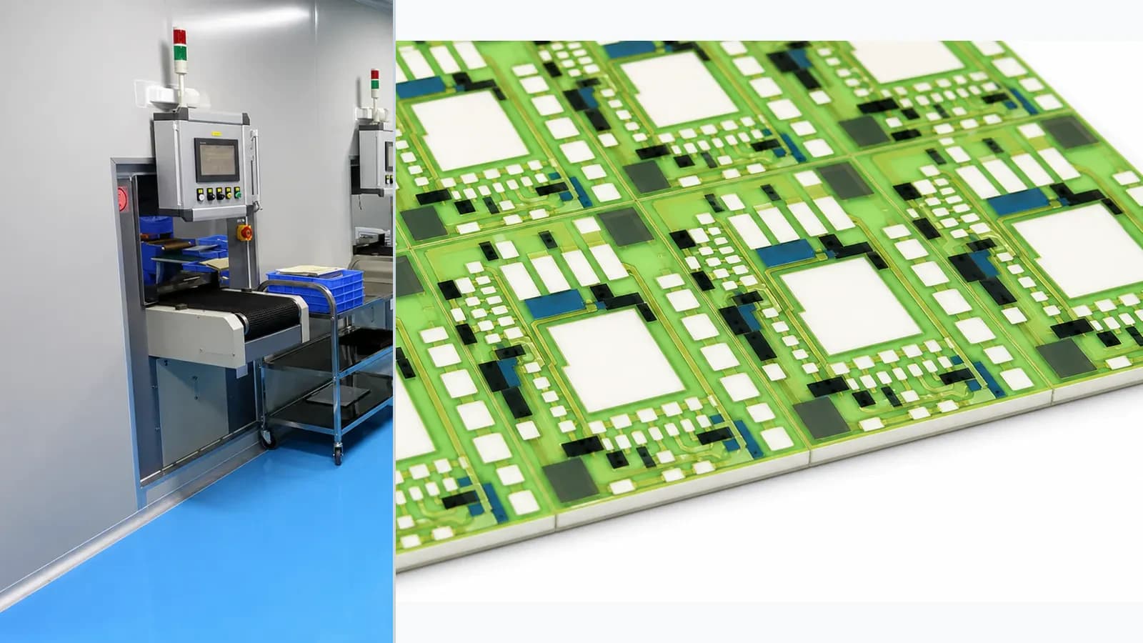
Overview
This process control record treats Thick Film Dielectric and Overglaze Processing as a controlled release sequence rather than a machine-list claim. It connects incoming inputs, process variables, inspection points, exceptions, and traceability to the failure each control prevents.
Control sequence
The order makes assumptions and ownership visible before a result is promoted to a requirement.
- 01
Release the input revision
For Thick Film Dielectric and Overglaze Processing, close remaining assumptions and link the quoted or released scope to the drawing revision, evidence set, owner, and change-control plan.
- 02
Confirm materials and tooling
For Thick Film Dielectric and Overglaze Processing, document the functional requirement, operating boundary, interfaces, quantities, and acceptance owner against the current drawing.
- 03
Control the process window
For Thick Film Dielectric and Overglaze Processing, complete control the process window against the controlled drawing, named assumptions, responsible owner, required evidence, and release decision.
- 04
Measure the critical output
For Thick Film Dielectric and Overglaze Processing, agree the inspection method, sample plan, acceptance criteria, traceability, and report format before validation.
- 05
Record exceptions and disposition
For Thick Film Dielectric and Overglaze Processing, complete record exceptions and disposition against the controlled drawing, named assumptions, responsible owner, required evidence, and release decision.
Engineering review matrix
Each row links a design variable to evidence that can support a drawing or release decision.
| Variable | Control question | Verification route |
|---|---|---|
| Voltage definition | For Thick Film Dielectric and Overglaze Processing, separate working, transient, test, common-mode, and fault voltages; identify polarity, waveform, duration, and source impedance. | Verify the released construction and method; do not infer a universal voltage rating. |
| Geometry | Spacing, creepage, clearance, edges, holes, crossovers, topography, and contamination paths must be visible in layout. | Inspect critical dimensions using defined datums and processed-part conditions. |
| Dielectric stack | Material, printed thickness, layer count, firing or cure, porosity, pinholes, and interfaces control isolation. | Measure processed thickness and defects, then correlate with construction-specific electrical testing. |
| Environment | Humidity, condensation, ionic contamination, chemicals, pressure, temperature, and altitude alter leakage and breakdown risk. | Condition specimens before and during bias or dielectric testing as required. |
| Failure response | Test energy, current limit, ramp, dwell, trip logic, re-test policy, and post-test inspection determine safety and meaning. | Record waveform, limits, result, specimen identity, and disposition. |
Failure controls
These are review prompts, not evidence that every risk applies or that every test is available.
- A
Surface leakage or tracking along contamination and protection interfaces
- B
Pinholes, voids, edge thinning, or topography reducing dielectric thickness
- C
Arc or breakdown at pads, edges, vias, cutouts, or damaged overcoat
- D
Latent damage from excessive test energy or undefined re-test policy
Inputs for a practical review
Unknown values may be labelled unknown. The review should convert uncertainty into an explicit decision or validation task.
Send Drawings- 01
Working, transient, fault, and test voltages with waveform and duration
- 02
Creepage, clearance, insulation, and leakage criteria
- 03
Complete conductor/dielectric/protection stack and geometry
- 04
Environment, humidity, altitude, contamination, and media
- 05
Test ramp, current limit, dwell, trip, and disposition