
On this page
Two lines can be close on a ceramic substrate but far apart along the resistor's electrical path. Capacitance between those lines bypasses the resistance between them, not necessarily the whole resistor. A correct DC value can therefore coexist with an unexpected fast output response. Start with the connected nodes and the receiving load before changing the serpentine layout.
System boundary
A folded printed resistor used as a loaded signal path in a ceramic hybrid. One dominant internal parasitic capacitance is modeled; external digital-aggressor injection and high-frequency distributed effects require their own circuit models.
Integration interfaces
| Interface | Required input | Thick film role | Validation owner |
|---|---|---|---|
| Adjacent physical folds | Electrical node order, potential distribution and overlap geometry. | Maintain the specified resistor routing and spacing. | Layout and circuit designer. |
| Resistor output to receiving load | Input resistance, capacitance, bias and operating states. | Define the resistor terminals and internal path. | Receiving-circuit owner. |
| Pulse source and measurement fixture | Edge rate, source impedance, probe loading and time window. | Provide a testable circuit boundary. | Signal-integrity test owner. |
Integration risks
| Risk | Control or verification | Validation owner |
|---|---|---|
| A local capacitance is modeled across the entire resistor. | Retain the two internal node identities in the schematic. | Circuit reviewer. |
| A DC resistance test is treated as a transient test. | Compare both loaded operating responses. | Application engineer. |
| A lumped model is extrapolated beyond its frequency range. | Check additional parasitics and measurement bandwidth. | Validation owner. |
System integration decisions
- Label adjacent folds by electrical position, not just physical spacing.
- Draw each significant capacitance between its actual nodes.
- Compare the loaded transient with the DC divider result before attributing all error to resistor value.
Follow the electrical path through the folded geometry
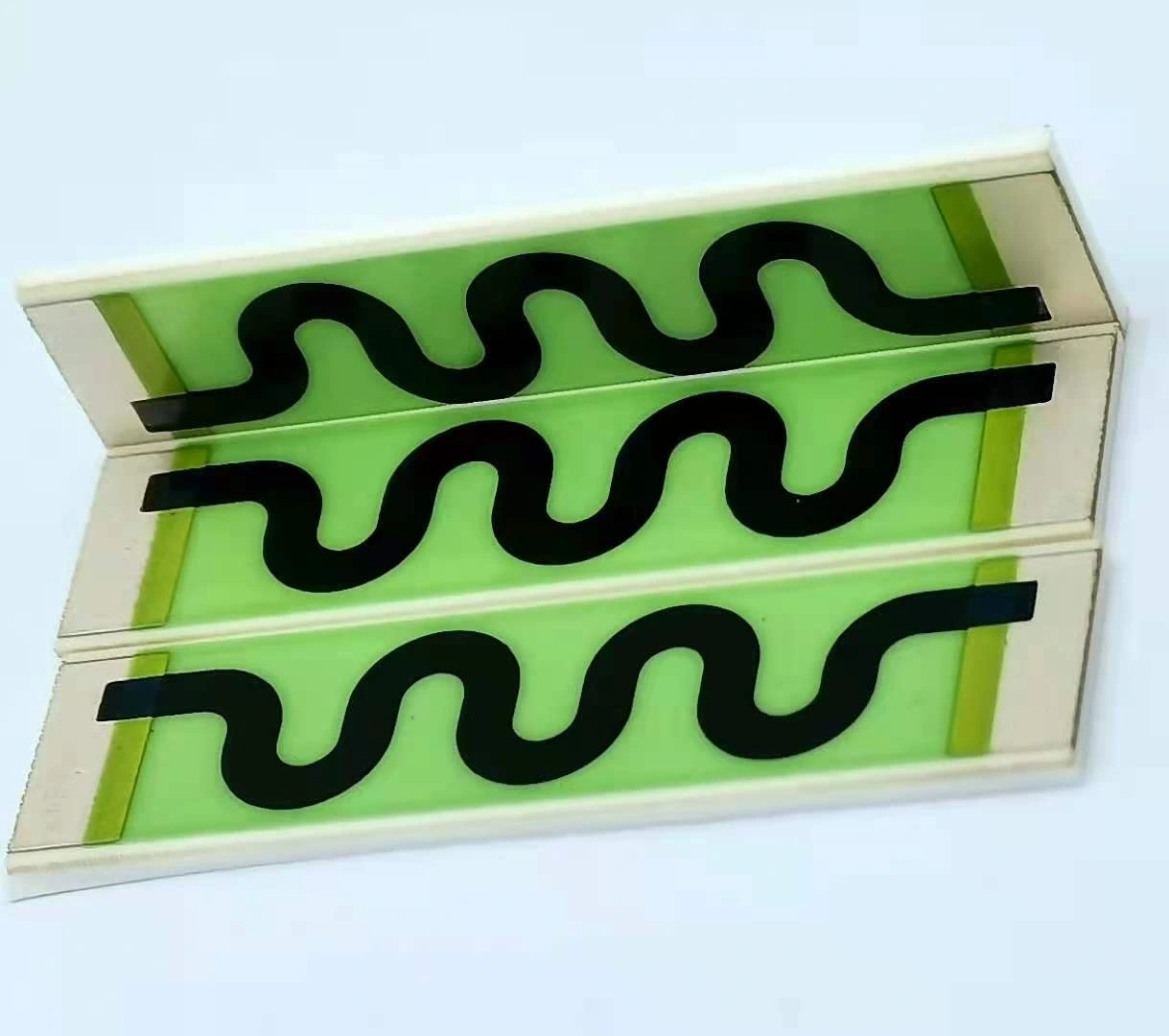
Mark the input and output, then number the turns along the resistive path. Highlight any pair of long adjacent runs whose node voltages differ appreciably in the intended circuit. A physically neighboring run may be several turns away electrically. That distinction determines which resistance lies between the two capacitor plates in a first-order equivalent circuit.
Do not infer capacitance from the green protective coating's appearance or from an image alone. Material stack, spacing, overlap, surrounding conductors and the installed environment all matter. The useful layout review is a connectivity map tied to a controlled drawing. A close photograph helps identify the features, but it cannot provide a reliable parasitic value without the geometry and electrical boundary.
Separate the section being bypassed from the sections that remain
Represent a simple path as Ra, Rm and Rb in series. A capacitance Cp bridges only Rm. The output drives a finite resistance RL to ground, and the input comes from an ideal voltage source for this calculation. Ra and Rb remain in the current path even when Cp increasingly bypasses the middle section. This topology is different from placing Cp between the two external resistor terminals.
The model is intentionally small enough to check against measurements. If several folds couple strongly, retain several internal nodes instead of forcing every capacitance into the same branch. If the neighboring conductor is an independent digital signal rather than part of this resistor, it is an aggressor port and must be driven separately. The internal shortcut model cannot answer that external crosstalk problem.
Calculate the response seen by the receiving load
The middle impedance is Rm divided by one plus s Rm Cp. Substitute that impedance into the loaded divider and multiply numerator and denominator by the same factor. The expression below preserves the middle-section bypass and the resistance that is never bypassed. It shows why a single total-resistance value is insufficient for a fast signal.
At low frequency the capacitor is effectively open and all three resistor sections contribute. Within this ideal lumped model, the upper-frequency plateau depends only on Ra plus Rb and the load. This plateau is not a prediction at arbitrarily high physical frequency: source impedance, other capacitances, inductance and distributed geometry eventually change the response.
H(s)=RL(1+sRmCp)/[(Ra+Rm+Rb+RL)+sRmCp(Ra+Rb+RL)]
- H(s): dimensionless output-to-input voltage transfer; s: complex frequency in reciprocal seconds.
- Ra, Rm and Rb: input-side, bypassed-middle and output-side resistance in ohms.
- RL: receiving load resistance to ground in ohms; Cp: capacitance bridging only Rm in farads.
Linear constant components, ideal input voltage source, one dominant internal capacitor, finite resistive load and negligible other parasitics. The expression is not a complete high-frequency material model.
The same nominal resistance can conceal different fast gains
As a hypothetical circuit example, take Ra and Rb as 10 kilohms each, Rm as 80 kilohms, RL as 10 kilohms and Cp as 20 picofarads. Total DC path resistance is 100 kilohms. The low-frequency gain is 10/110, approximately 0.090909. The internal shortcut model approaches 10/30, approximately 0.333333, while its assumptions remain applicable.
The numerator zero is about 99.47 kilohertz. The denominator pole is about 364.73 kilohertz because the effective time constant is Rm Cp multiplied by 30/110. If the same numerical capacitance were mistakenly drawn across the entire 100-kilohm resistor, the model would instead approach unity gain. That substantial difference comes from topology, not a change in the resistor's DC tolerance.
Use the transient shape to challenge the node assignment
For an ideal input step from a settled zero state, the illustrative internal-shortcut model initially transfers one third of the step and then settles to one eleventh. Its exponential time constant is approximately 0.436364 microsecond. The initial capacitor voltage remains continuous; the ideal source step redistributes voltage around the bypassed middle section without making its capacitor voltage jump.
A real source has finite rise time and impedance, so its observed edge will not necessarily show those exact initial and final levels. Use the calculation to identify a testable shape and scale, then include the actual source and receiving input in the model. A logic threshold crossed by the early excursion can matter even when a slower instrument reports the correct settled divider value.
Choose the experiment that distinguishes the competing models
Keep the same receiving load while comparing a slow sweep, a faster sweep and a controlled pulse. Changing the load changes the transfer and may obscure the difference being investigated. Record the measurement probe and fixture capacitance because adding a probe to an internal node creates a new branch that may be comparable to the parasitic under study.
The following comparisons separate three different engineering questions. They should not be combined into one generic high-frequency checklist. A failed external-noise test calls for the aggressor waveform; an internal shortcut calls for the segment topology; a DC layout problem calls for resistance distribution and current density. Each has a different corrective action.
| Connection or observation | Model to retain | Useful verification |
|---|---|---|
| Capacitance bridges a middle resistor segment | Ra–(Rm parallel Cp)–Rb with real load | Loaded gain and transient shape |
| Capacitance spans the external terminals | Entire resistor parallel Cp | End-to-end impedance and receiving load |
| Nearby digital conductor drives a separate node | Independent aggressor source and coupling branch | Edge-driven victim response |
| DC value or local heating changes at a turn | Resistive geometry and current distribution | DC measurement and thermal/layout review |
Change the geometry only after locating the influential coupling
A layout change can separate high-voltage-difference runs, alter the order of neighboring sections or reduce a long overlap. Evaluate the resulting resistor area, conductor routing and process constraints at the same time. Increasing every gap without identifying the influential node pair may enlarge the part while leaving the relevant coupling through another conductor essentially unchanged.
Do not promise a capacitance reduction from a spacing ratio unless the actual field geometry supports that approximation. Conductive surroundings and overlying features can dominate the field. Compare candidate layouts using an appropriate extracted model or measured representative structures, and preserve the circuit load and source conditions so the resulting improvement has a clear electrical meaning.
Send a node-marked layout with the required signal result
Provide the resistor drawing with segment order, accessible terminals, adjacent conductors and the suspected coupling nodes marked. Include the total and segment resistance assumptions, the receiving input model, pulse amplitude and edge range, and the allowable output excursion or settling requirement. State whether any internal node can be measured without changing the assembled circuit.
The useful acceptance output is a comparison between the intended signal and the loaded measured response under defined conditions. Keep the DC resistance record alongside it, rather than replacing one test with the other. This allows the printed resistor network and the complete electronics assembly to be improved at their actual interfaces, without asking a resistance trim to correct an incorrectly connected parasitic model.
Send the folded-path signal definition
Include internal node order and the receiving load, not only nominal resistance.
- Node-marked serpentine drawing and nearby independent conductors.
- Total/segment resistance assumptions and supported parasitic estimates.
- Source rise time, impedance, pulse range and actual receiving circuit.
- Required excursion/settling result and controlled measurement configuration.
The drawing-upload form loads as you reach this section.