
On this page
- 1960s: thick film becomes a production route for hybrid circuits
- 1970s–1980s: material systems broaden and process control matures
- Multilayer ceramic routes move conductors inside the substrate
- Polymer thick film brings printing to temperature-sensitive substrates
- Pastes become functional sensors and thermal elements
- The continuing trend is lower temperature with tighter integration
- What has not changed
Prepared by Chipsimple Engineering Team, Engineering and technical content review
Published online August 9, 2026 · Reviewed August 9, 2026
Source and scope: This article is a technically reviewed English edition of a December 2024 company-engineer note. Company rankings and market-size claims in the source were omitted because they were not supported by dated primary evidence. The history below focuses on documented technology changes rather than promotional firsts.
Electronic paste became important when circuit makers needed repeatable functional films without machining every conductor and resistor as a separate part. A paste could carry metal, conductive oxide, glass, ceramic, or carbon through a patterned printing process. Drying and thermal processing then converted that deposited shape into an electrical layer. The method made passive networks and interconnects practical on ceramic long before “printed electronics” became a broad industry label.
1960s: thick film becomes a production route for hybrid circuits
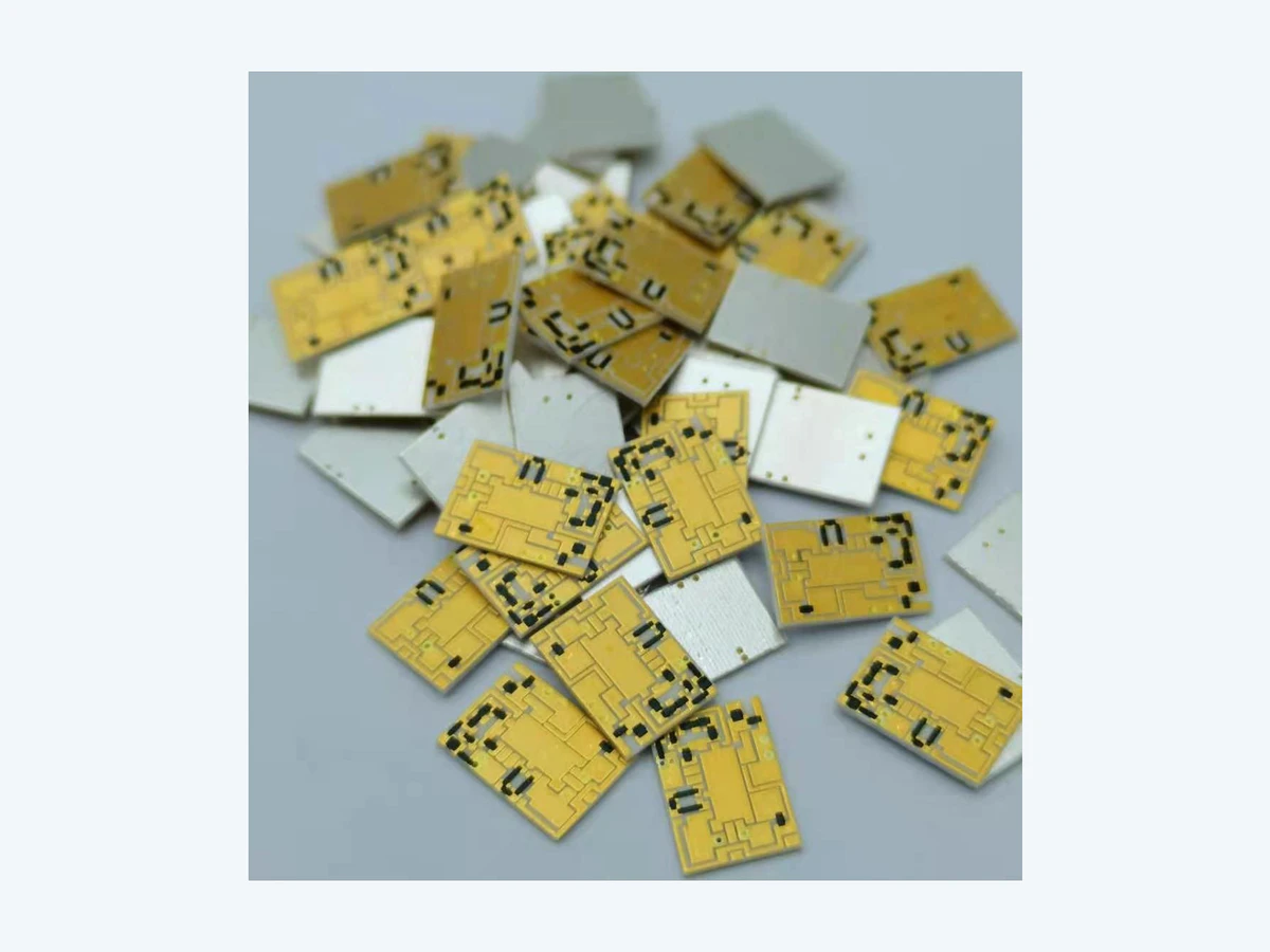
IEEE’s technology history places the emergence of thick-film electronics in the 1960s, when screen-printed conductors, resistors, and dielectrics offered a cost-effective route to passive networks and interconnects in hybrid integrated circuits. The hybrid combined printed passives on an insulating substrate with separately attached semiconductor devices.
The core paste architecture was already recognisable: a functional phase for electrical behaviour, an inorganic bonding phase where the fired system required it, and an organic vehicle that made the composition printable. Alumina became a common platform because it combined electrical insulation, mechanical stability, and compatibility with established air-fired material systems.

1970s–1980s: material systems broaden and process control matures
As hybrid production expanded, paste suppliers developed conductor families for soldering and wire bonding, resistor decades with different TCR and stability behaviour, multilayer dielectrics, overglazes, and specialised terminations. Laser trimming became a production method for bringing fired resistors from an as-fired distribution to final value.
Material compatibility became as important as the individual paste property. A conductor had to retain adhesion and attachment performance after later firing. A dielectric needed insulation and pinhole control without damaging adjacent conductors. A resistor required stable interfaces and predictable response to refiring and trimming. Supplier families and process guides emerged because a list of ingredients could not control those interactions.
Multilayer ceramic routes move conductors inside the substrate
High-temperature co-fired ceramic and later low-temperature co-fired ceramic extended printing from a surface operation to three-dimensional ceramic interconnect. Conductors and via fills could be printed on green tape, stacked, laminated, and co-fired. Refractory metals such as tungsten or molybdenum served high-temperature ceramic routes; precious-metal and copper systems became associated with other co-fired families.
Kyocera’s description of high-alumina packages shows tungsten metallization printed between green ceramic layers and co-fired above 1500 °C in a controlled atmosphere. Modern LTCC routes operate differently and use their own tapes and conductors. The historical significance is the same: electronic paste became part of the ceramic body, not only a film on its surface.

Polymer thick film brings printing to temperature-sensitive substrates
Polymer-bound silver, carbon, dielectric, and resistive inks enabled functional circuits on polyester, polyimide, FR-4, glass, and formed parts at temperatures below ceramic firing. These materials supported membrane switches, flexible tails, printed contacts, sensor tracks, heaters, and later in-mould electronics.
The lower process temperature did not make the engineering simpler. Substrate treatment, solvent compatibility, cure, adhesion, flexibility, abrasion, humidity, silver migration, forming, and connector interfaces became central. A cured polymer conductor is not a low-temperature version of a fired ceramic conductor; it is a different material system.
Pastes become functional sensors and thermal elements
Printed resistive materials can be designed as fixed resistors, position-sensor tracks, level-sender cards, temperature-dependent elements, strain-sensitive layers, or heaters. The same screen-printing method now serves very different measurements and loads.
A sensor track is judged by curve, contact resistance, wear, media exposure, and life. A heater is judged by resistance distribution, dielectric insulation, watt density, heat spreading, mounting, controls, and abnormal-condition response. A precision network emphasises ratios, TCR tracking, trim stability, and voltage stress. Paste development followed these functions rather than one straight path toward higher conductivity.

The continuing trend is lower temperature with tighter integration
Current development includes finer printed features, lower-temperature cure and firing, higher-conductivity paths, flexible and stretchable substrates, printed component attachment, environmental durability, and reduced precious-metal use. At the same time, legacy fired thick-film systems remain valuable because they provide stable, compact functional layers on ceramic across long-established supply chains.
“Newer” does not mean “better” without an application. A polymer conductor may suit a flexible sensor but fail a high-temperature ceramic assembly. A gold conductor may support a bonding requirement but add cost where silver is adequate. A copper system may offer conductivity and material economics but demand atmosphere and compatibility controls. Technology selection still starts with the full use condition.
A practical timeline
| 1960s | Screen-printed passive networks and interconnects become established in hybrid microelectronics. |
|---|---|
| 1970s–1980s | Broader conductor, resistor, dielectric, overglaze, attachment, and laser-trim material systems mature. |
| Multilayer era | HTCC and LTCC move printed conductors and vias into laminated ceramic structures. |
| Polymer expansion | Low-temperature cured inks support membrane circuits, flexible interconnects, contacts, sensors, and formed electronics. |
| Functional integration | Printed resistive and dielectric layers become engineered sensing, heating, power, RF, and packaging elements. |
| Current direction | Finer geometry, lower process temperature, flexible form factors, reliability modelling, and material-efficiency work continue alongside mature ceramic routes. |
What has not changed
- The paste is part of a material stack, not a stand-alone ink choice.
- Printed geometry and rheology are linked to finished electrical performance.
- Drying, curing, or firing must be defined by the selected material system.
- Supplier typical values require the stated specimen and process conditions.
- Assembly, environment, and inspection belong in the design before production release.
The vocabulary has expanded from hybrid circuits to printed electronics, but the engineering discipline remains recognisable: define the function, select compatible materials, control the deposited geometry and thermal history, then validate the finished part under its real use conditions.
Primary references
- IEEE Technology Navigator, Thick films — historical and technical overview of thick-film functional layers and their emergence in 1960s hybrid electronics.
- Kyocera America, Thermal Conductivity of Thick Film Tungsten Metallization used in High-Alumina Ceramic Microelectronic Packages — a manufacturer-authored description of green tape, refractory metallization, lamination, co-firing, and plating.
- Heraeus Electronics, Thick Film Materials — current functional categories illustrating how conductor, resistor, dielectric, polymer, and specialised paste systems have diversified.
Choose a present-day route from the actual requirement
Send the function, substrate, layer drawing, electrical and thermal loads, assembly, environment, quantities, and validation needs. The review can compare fired ceramic, polymer, multilayer, sensor, and heater routes without assuming that one technology replaces the others.