
On this page
Prepared by Chipsimple Engineering Team, Engineering and technical content review
Published online August 10, 2026 · Reviewed August 10, 2026
ENGINEERING ARTICLE 25 / VOLUME 5
Soldering, Wire Bonding or Conductive Adhesive: Choosing the Assembly Interface
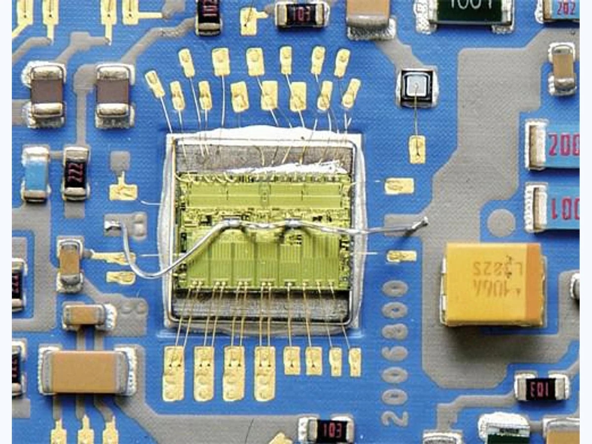
The assembly method is not a final purchasing choice; it shapes pad metallurgy and layout from the beginning. Solder creates a metallic joint through a thermal cycle, wire bonding creates a small solid-state interface under local force and energy, and conductive adhesive cures a particle-filled polymer layer. Each method transfers current and mechanical load differently.

Select from Electrical and Thermal Duty
Joint resistance, current density and operating temperature set the basic interface need. The consequence is practical: a low-level sensor bond and a power terminal need different area and stability. This is one reason ceramic circuit assembly methods cannot be reduced to a single catalogue value.
During design review, state continuous and pulse current, voltage, temperature and heat flow. The objective is not to freeze every process setting on the customer drawing, but to define the functional boundary that the manufacturer must protect.
A useful evidence package contains joint resistance and temperature rise before and after ageing. Comparing those records with the approved construction is more informative than judging an isolated photograph or one resistance reading.
Watch for using a convenient low-current interface on a power path. It often indicates that two individually acceptable variables have combined at the edge of their windows.
Match Metallurgy to the Joining Process
Pad surface must wet, bond or adhere with the chosen material. Consequently, solder can leach conductor, wire bonds can reject contaminated surfaces and adhesive can be sensitive to oxide or roughness. The engineering value comes from understanding the direction and sensitivity of the effect, not from memorising a nominal number.
A robust drawing or process plan will qualify pad stack with alloy, wire or adhesive product. This makes the design intent visible and gives the supplier room to use a qualified material set without changing the function.
The result can be checked through pull, shear, wetting or contact-resistance distributions. Where possible, keep readings before and after the next thermal or mechanical operation; the delta often reveals more than the final value.
The failure pattern to investigate is good appearance with weak or unstable electrical contact. Before changing materials, confirm orientation, lot history, measurement method and acceptance limits.
Manage Heat and Process Exposure
The physical starting point is straightforward: Joining thermal cycles can refire, stress or contaminate printed films. From there, temperature-time and flux or cure chemistry affect adjacent resistors and dielectrics. For ceramic circuit assembly methods, the important issue is the amount of process margin left after normal variation is included.
On the drawing and in the review record, define profile, allowable repeats and cleaning. Keep the requirement functional wherever possible, while making any safety- or interface-critical boundary unambiguous.
A production trial should capture electrical values before and after assembly simulation. Record the condition of the specimen and the next operation so that a later change can be traced to a specific stage.
If the team sees resistor drift or dielectric leakage introduced after final circuit inspection, pause before adding inspection or rework. First check whether the layout and the qualified process window are asking for contradictory outcomes.
Design Mechanical Compliance
In a stable manufacturing route, rigid terminals and large joints transfer CTE strain to ceramic pads. This means a strong joint can still peel conductor or crack ceramic. The observation is especially useful because it connects a visible feature to an electrical, thermal or mechanical consequence.
The control plan should use compliant leads, controlled bond area and strain relief. It should also name the drawing characteristic or coupon that represents the requirement, avoiding an instruction that depends on personal interpretation.
Evidence comes from mechanical and thermal-cycle testing on the full joint geometry. A trend across position or lot is usually more valuable than a perfect reading from one hand-picked sample.
Investigate pad lift at the edge of a stiff attachment. The pattern may identify a narrow process interaction long before the final circuit becomes an open, short or out-of-tolerance value.
Control Cleanliness and Storage
A useful way to frame the decision is this: Bond and solder surfaces change with handling and time. As a result, fingerprints, oxidation, absorbed moisture and expired adhesive reduce consistency. That cause-and-effect chain should remain visible when ceramic circuit assembly methods is reviewed with purchasing and quality teams.
The manufacturing boundary is protected when the team can set packaging, shelf life, conditioning and time-to-join. This approach separates the customer's functional need from the supplier's machine-specific compensation.
Confirm the decision with surface checks and periodic process-control specimens. Include both typical and boundary-condition specimens where the failure consequence justifies them.
The symptom assembly yield changing by storage history rather than circuit lot deserves a structured investigation. Check material lot, artwork position, thermal history and measurement setup before assigning a single cause.
A Worked Engineering Review
A ceramic module needs fine signal connections and two power terminals. Gold or aluminium wire bonding may suit the signal pads when the conductor stack is qualified, while solder or a mechanically supported terminal may serve the power path. Conductive adhesive could reduce peak assembly temperature but introduces cure, thickness and ageing controls. The engineer should not select one method for visual uniformity. Separate pad families and coupons let each interface be optimised and tested.
Design Review Checklist
- Map electrical and thermal duty per joint.
- Qualify pad and joining metallurgy together.
- Control profile, cure and cleaning.
- Provide compliance and strain relief.
- Test aged joint resistance and strength.
Questions Engineers Commonly Ask
Is conductive adhesive a drop-in replacement for solder?
No. It has different contact, cure, moisture, mechanical and ageing behaviour. The pad and joint geometry must be qualified.
Can any gold pad be wire bonded?
No. Surface chemistry, roughness, thickness, cleanliness and underlying adhesion matter.
Which method is best for high temperature?
It depends on the exact temperature, current, atmosphere and materials. Compare the complete qualified joint, not the generic method name.
Related Engineering Resources
Closing Note
Choose the assembly interface with the same discipline used for printed layers. Pad metallurgy, joining process, mechanical load and qualification evidence belong in one controlled construction.