
On this page
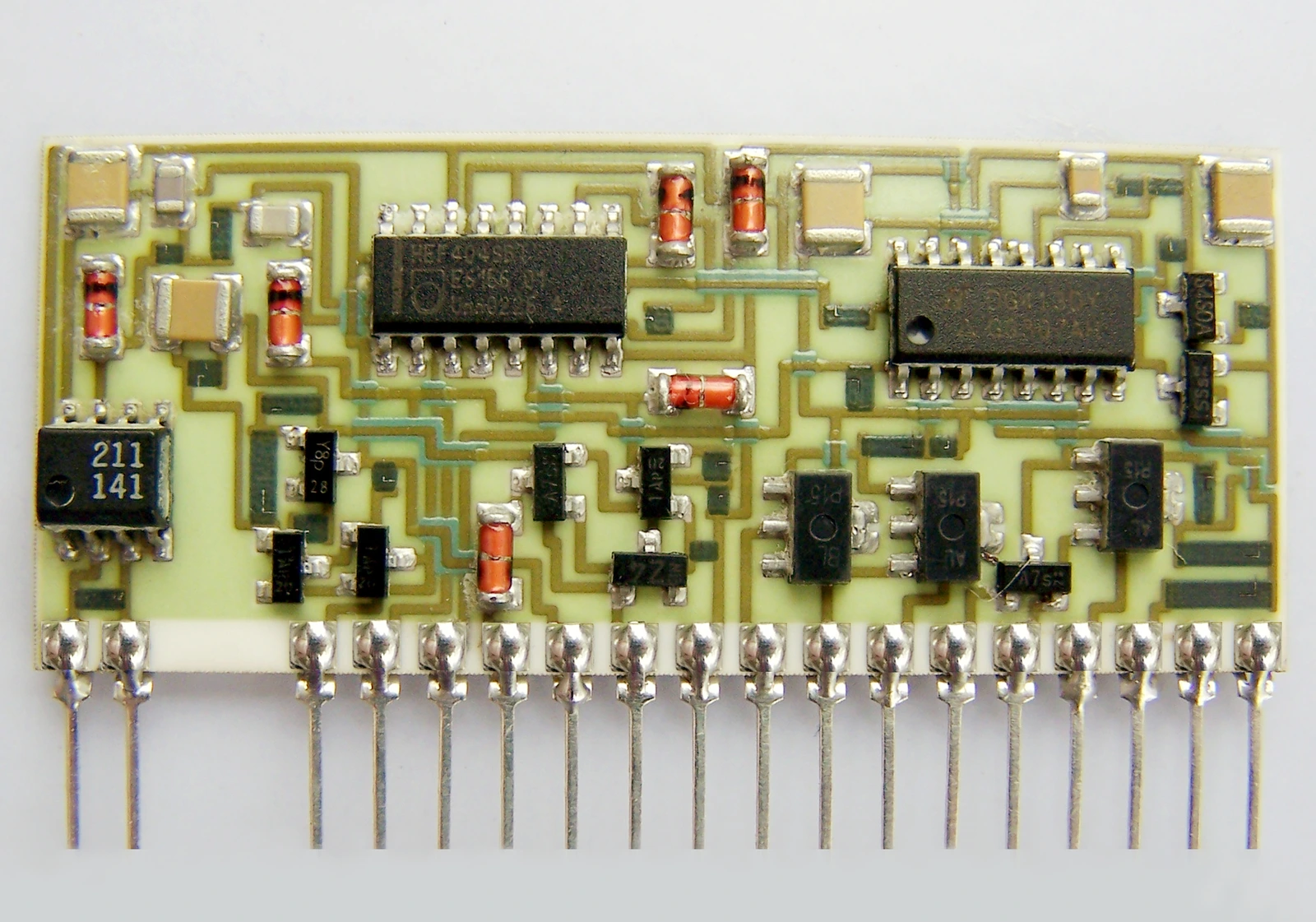
A component that points left in the assembly drawing may point upward in a rotated inspection image. That visual difference is not a polarity error. The check must connect the component's actual terminal or polarity mark to the correct circuit pad in a defined board coordinate system. This is especially important on repeated ceramic panels where neighboring cells can be intentionally rotated while carrying similar-looking components.
Measurement purpose
Verify polarity independently of board and camera orientation.
Specimens and conditions
- Board frame
- Inspected face, asymmetric landmark and cell transforms defined.
- Component identity
- Exact approved package and marking convention available.
Equipment and records required
- Visual inspection: Resolution sufficient to identify the actual polarity discriminator.
- Mapping verification: Independent physical witness or approved electrical method for the relevant node mapping.
Method sequence
- Identify
Verify board frame, component type and location.
Record: Designator and orientation map.
- Compare polarity
Relate physical mark to the required circuit pad.
Record: View-indexed result.
- Challenge
Check permitted rotations and ambiguous marks using independent evidence.
Record: Witness outcomes and disposition.
Decision and uncertainty
Accept only the mark-to-pad relation defined for the exact component and view.
Hidden marks and parallel electrical paths can leave identity unresolved.
Assembly drawing and test-method owners.
Traceable outputs
| Record | Required contents |
|---|---|
| Polarity map | Component, mark, pad and local orientation. |
| Inspection evidence | Images, visibility limits, independent checks and correction history. |
Method review decisions
- Identify the printed face and board landmark before interpreting component marks.
- Use the actual component manufacturer's marking convention, not a universal stripe rule.
- Verify the mark-to-pad relationship in local board coordinates rather than screen-left or screen-right.
Establish the board frame before inspecting components
Choose an asymmetric ceramic or printed landmark that identifies the inspected face and orientation. State the direction of the board axes and the location of the origin on the inspection drawing. A rectangular outline alone often permits a half-turn ambiguity. A hole pattern, keyed edge or controlled fiducial may resolve it, but only if the drawing assigns that feature the required relationship.
Keep panel orientation separate from individual cell orientation. A panel can contain cells rotated relative to one another for manufacturing reasons. The camera's global coordinates therefore do not necessarily describe each component's local orientation. Record the cell transform explicitly rather than asking an inspector to remember which rows should look reversed.
Decode the component mark from its exact part record
Use the approved component part number, package drawing and marking information. A stripe, dot, bevel or chamfer can indicate different things on different packages. Some bidirectional protection devices have no polarity band even though a related unidirectional device does. Do not generalize from a familiar diode or assume that every visible line identifies a cathode.
Separate a polarity mark from a manufacturer logo, lot code or molded feature. If the marking is partly covered by coating or attachment material, identify another approved discriminator or place the inspection before that feature becomes hidden. Guessing from a blurred mark is not a valid substitute for the package definition. Retain the source revision used for the interpretation internally.
Write the required mark-to-pad relationship
For each polarized component, identify the relevant terminal and the circuit node it must contact. Describe the relationship using component designator, pad identity and the board landmark. An instruction such as band toward the keyed hole is more reproducible than band to the left, provided the key and pad relationship are controlled and unambiguous.
Do not rely only on the placement angle in an assembly machine file. Package-zero conventions can differ between libraries or suppliers. Verify the physical mark on a known correctly identified specimen against the receiving footprint and circuit graph. Keep pad numbering, component pin numbering and the machine's rotation convention as separate fields until their mapping has been verified.
Transform the view without changing polarity
Assume an illustrative component's marked end lies along the positive x direction in board coordinates. For this example both board and displayed Cartesian axes have x to the right and y upward. Rotating the displayed board 90 degrees counterclockwise maps that direction to positive image y. Many camera pixel systems instead have y increasing downward: the same displayed upward direction is then negative pixel y. Declare the convention before implementing the transform. The component remains correct when its marked end connects to the required physical pad, not when it satisfies a screen-left rule.
For a 180-degree view rotation, the same board direction appears reversed in the image. A mirrored back-face view is not equivalent to either rotation and must use a separately defined transform. Test the mapping with an asymmetric witness so an image-processing setting that silently mirrors the camera cannot reverse the polarity decision.
| Viewing transformation | Board +x appears as | Polarity decision |
|---|---|---|
| No in-plane rotation | Image +x in either stated convention | Compare mark with mapped pad |
| 90° counterclockwise, Cartesian y upward | Image +y | Same physical pad remains required |
| 90° counterclockwise, pixel y downward | Pixel −y | Convert axes before comparing coordinates |
| 180° rotation | Image −x | Do not use screen-left rule |
| Opposite-face mirrored view | Depends on declared reflection axis | Use explicit face transformation |
Check identity, location and polarity in that order
First verify that the component is the approved type and belongs at the stated designator. Next confirm that it occupies the intended pads. Then inspect polarity using the defined relationship. A correctly oriented wrong component can pass a polarity-only check; a correct component placed on the wrong pair of pads can do the same.
Record missing, unreadable and ambiguous marks separately from confirmed reversals. These require different dispositions. A missing mark may call for another identification method; a confirmed reversed part requires the authorized assembly process to decide correction. Do not energize an uncertain assembly simply to see whether it works, especially when reverse connection can damage the component or create a hazardous circuit state.
Use electrical checks as complementary evidence
A suitable unpowered electrical check can support a polarity investigation, but the connected circuit may contain parallel paths, protection devices or active components. Define the test nodes and safe stimulus before interpreting a diode-mode reading. A forward-like reading between two external terminals does not automatically prove which physical component produced it.
Where visual and electrical evidence disagree, preserve both and inspect the mapping chain. The error may be in the component installation, fixture wiring, drawing view or test program. Reversing test leads until a familiar value appears does not resolve that ambiguity. Use a known connection reference and the complete circuit topology to choose the next discriminating observation.
Challenge the map with rotations and deliberate exceptions
Validate the inspection method using clearly identified nonproduction witnesses or approved reference assemblies. Include each permitted board orientation, a rotated cell, a missing component and a deliberately represented polarity error. The purpose is to show that the method detects the relationship rather than memorizing one attractive reference image.
Repeat the relevant challenge after a camera mirror setting, fixture orientation, component supplier package or footprint library changes. Keep the expected result for each witness before running the check. A perfect result on a full panel in one orientation does not establish correct interpretation after a partial reload or a change to a visually similar component package.
Deliver a polarity map that survives a changed viewpoint
The final map should link designator, exact component identity, polarity discriminator, required pad and local cell orientation. Store the actual inspection view and any visibility limitation with the result. This gives assembly and inspection teams one recoverable relationship instead of competing left/right descriptions.
For a hybrid integrated circuit or populated ceramic module enquiry, send the schematic, assembly drawing, component package definitions and permitted inspection access. ChipSimple can review the drawing-specific ceramic circuit and assembly interfaces. Polarity verification complements placement, joint and functional checks; it does not establish overall assembly reliability or authorize changes to a safety-relevant system.
Send the assembly and polarity definitions
Include the local board view and exact package rather than only a machine placement angle.
- Schematic nodes, pad numbers and component designators.
- Manufacturer package and marking records for approved parts.
- Panel/cell orientation, camera face and asymmetric landmarks.
- Inspection access, ambiguous images and permitted electrical checks.
The drawing-upload form loads as you reach this section.