
On this page
A connector can mate mechanically while its signals are assigned to the wrong contacts. The risk is greatest when one drawing shows the mating face, another shows wire entry, and a ceramic layout numbers pads from its own viewing direction. A pinout review must preserve the identity of each physical cavity through those views. Left-to-right order and a readable label are not reliable substitutes for that mapping.
Measurement purpose
Verify the physical cavity-to-net relationship across connector views, harness data and ceramic terminals before accepting an electrical interface definition.
Specimens and conditions
- Connector identity
- Exact housing variant, contact arrangement and current manufacturer drawing
- Circuit identity
- Current schematic, ceramic pad labels and harness or assembly mapping
Equipment and records required
- Orientation review: Identified physical connector or suitable model showing asymmetric housing features
- Electrical verification: An independently mapped mating fixture and excitation appropriate to the circuit topology
Method sequence
- View definition
Identify mating face, wire-entry view and cavity witnesses
Record: Orientation record
- Net mapping
Trace every populated and unpopulated cavity to its required function
Record: Cavity-to-net table
- Independent check
Challenge mirrored or shifted assignments with distinguishing electrical relationships
Record: Verified connection results
Decision and uncertainty
Accept only when manufacturer cavity identities, intended nets, ceramic pads and the actual test mapping agree.
Ambiguous views or symmetric electrical tests leave the mapping unresolved; they do not justify a guessed pinout.
The circuit and assembly design authorities own net assignment; the reviewer verifies its implementation.
Traceable outputs
| Record | Required contents |
|---|---|
| Interface map | Housing identity, face definition, cavity names, contacts, pads, nets and unused positions |
| Verification record | Independent fixture map, excitation, measured relationships and resolved conflicts |
Method review decisions
- Identify the exact connector and viewing face.
- Map physical cavities to named nets before tracing artwork.
- Verify asymmetric features and electrical relationships independently.
Keep cavity, terminal and net names separate
A cavity number identifies a location in a housing. A terminal part number identifies a contact component. A net name identifies an electrical function. These three labels can appear together but are not interchangeable. A change from pin to socket contacts may preserve the cavity numbering while changing the mating component, and a wire colour may change without changing the net.
Create one row per physical cavity. Record the housing part number and revision, cavity identifier, installed contact, wire or ceramic pad connection and net function. Include unpopulated positions rather than omitting them. An apparently empty cavity can be an important orientation witness and may prevent a shifted assignment from looking like a valid shorter connector.
Define the viewing direction with the housing features
State whether the drawing looks into the mating interface or toward the wire-entry side. Show the latch, key, polarization feature or another asymmetric physical detail in the same view. Different connector families can use different numbering arrangements; do not invent a universal rule that pin one is always at the left when the latch is above it. Use the exact manufacturer’s drawing.
A view from the opposite side often reverses apparent horizontal order, but an additional rotation changes the result again. The reviewer should reproduce the stated viewing operation on the identified housing or a trustworthy model. Copying a picture into a document and flipping it without preserving the face label can make its printed numbers look plausible while disconnecting them from the actual cavities.
Build a cavity-to-net table before checking conductor shapes
Trace the required electrical path from the mating contact to the ceramic terminal and onward to the intended circuit node. For a resistive sensor, distinguish excitation, return and wiper output. For a heater, distinguish power terminals from a separate sensing or protective circuit. A symmetric two-terminal resistor can conceal a reversed connector assignment that would be unacceptable for another circuit on the same assembly.
Use stable names in the table. If the customer schematic uses P1 and the assembly drawing uses J1, document their relationship instead of silently renaming one. Multiple aliases are manageable when they resolve to one physical interface; they become hazardous when two reviewers assume the same label means different ends of a harness.
Use an asymmetric witness to expose a mirrored assignment
Consider an illustrative four-cavity row viewed at the mating face, with a key beside cavity one. The intended functions are supply, output, return and unused. Viewed from the wire-entry side without another rotation, the apparent left-to-right order reverses, but the physical cavity identities do not change. The unused end position and the key provide witnesses that a symmetric pair of power contacts would not.
The example is a checking method, not a pinout for any named connector. Verify the real numbering in the applicable drawing. If the housing lacks visible identifiers, establish an approved orientation view before assigning functions. Never infer a production pinout solely from the order of wires in an attractive photograph.
| Physical cavity | Required function | Checks that must agree |
|---|---|---|
| 1 | Supply | Manufacturer cavity identity, key position, harness connection and ceramic supply pad |
| 2 | Output | Schematic node and actual receiver signal path |
| 3 | Return | Return net identity rather than assumed chassis ground |
| 4 | Unused | No unintended conductor, contact or test-fixture bridge |
Test the mapping without damaging the circuit
A continuity test should exercise the actual mating interface where practical, not only exposed ceramic pads. The fixture itself needs an independently verified cavity map. A harness and a test fixture built from the same mirrored drawing can agree with each other while both disagree with the customer interface. Use a known cavity witness or independently checked connector breakout to challenge that possibility.
Choose test excitation appropriate to the assembled circuit. An arbitrary buzzer threshold can be unsuitable for a printed resistor, protection component or high-impedance sensor path. Record the expected relationship for each tested pair, including intended resistive connections and required isolation. De-energize and make the setup safe under the responsible procedure before applying an external test signal.
Challenge cases in which the wrong mapping still appears correct
End-to-end resistance can remain unchanged when a symmetric resistor’s terminals are exchanged. A divider tested only at its middle position may also look correct after supply and return are swapped. Check an asymmetric operating position or another independent relationship that distinguishes the candidate mappings. The test must be selected from the actual topology, not copied from a generic connector checklist.
Shared returns can hide additional mistakes. Two cavities tied together in one harness variant may be separate in another, so a test on the first variant does not prove the second. Preserve connector variant, harness identity and any intentional bridges. A pass record without those conditions can be wrongly reused for an assembly whose cavity functions differ.
Resolve conflicts at the interface authority
When the schematic, housing drawing and pad layout disagree, identify the exact cavity and net involved. Provide the conflicting views side by side with their orientation labels and ask the responsible design authority to choose the intended connection. Do not resolve the issue by moving artwork until the connector matches an unapproved interpretation.
The approval should state the physical mapping, not merely say use the latest drawing. That wording can leave two independently revised files in conflict. After resolution, update the schematic, assembly view, artwork connection and test-fixture definition as applicable. A revision-control process then carries the change forward; it does not replace the initial electrical decision.
Retain the mapping that a second reviewer can reproduce
The final package includes the identified connector drawing, an unambiguous viewing face, the cavity-to-net table, ceramic terminal labels and a verified test connection map. Preserve an asymmetric witness photograph or model view where permitted. The useful record allows another reviewer to begin at a physical cavity and arrive at the same circuit node without relying on memory.
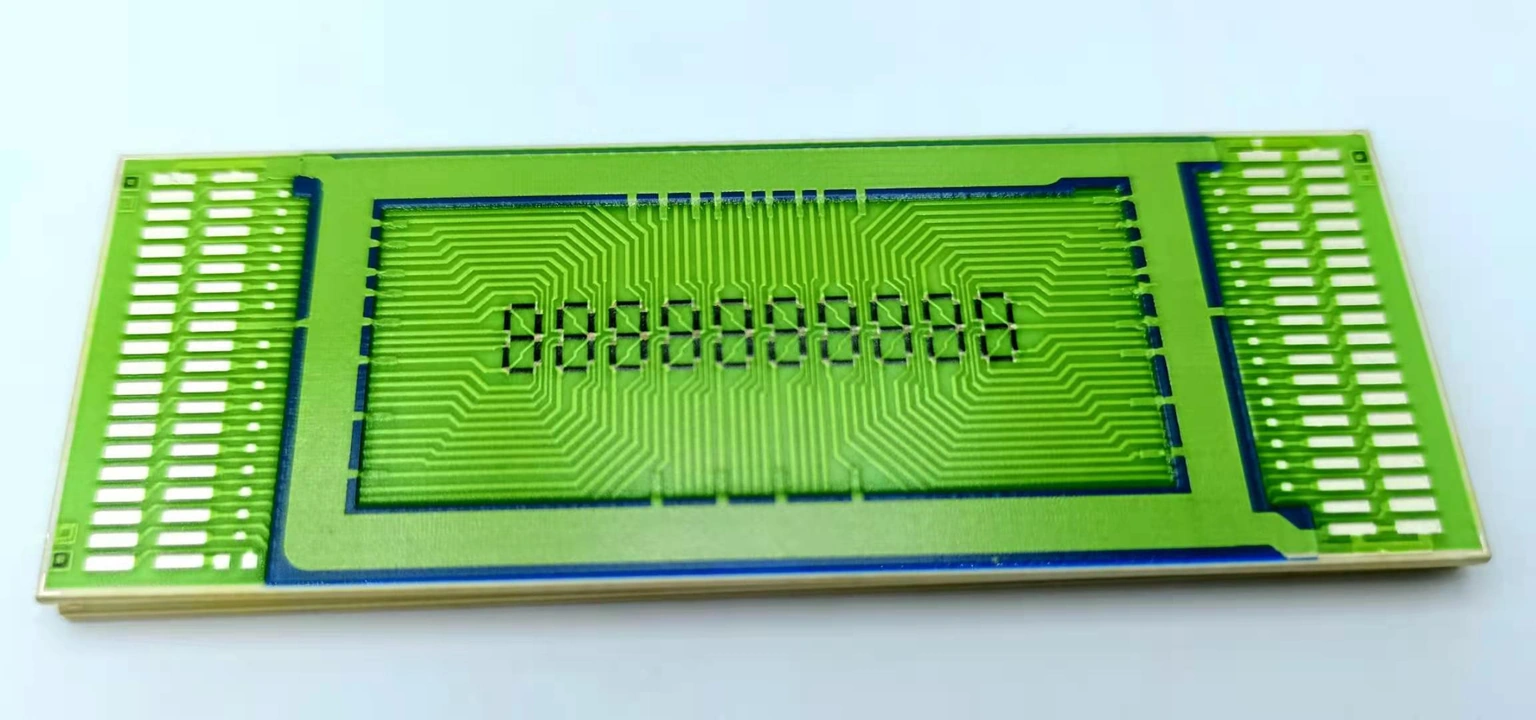
ChipSimple can review drawing-defined ceramic pads, conductor routing and terminal interfaces. Connector selection, harness function and system-level electrical approval remain with the designated assembly and circuit authorities. This separation prevents a correct ceramic pattern from being blamed for a mirrored harness and prevents a plausible continuity result from becoming an unsupported system approval.
Supply an unambiguous connector interface
Include the physical viewing information with the electrical schematic.
- Exact connector housing and mating-part drawings
- Mating-face and wire-entry views with latch or key visible
- Cavity-to-net table including unused positions
- Ceramic pad labels and required electrical relationships
- Harness variant and independently verified test-fixture mapping
The drawing-upload form loads as you reach this section.