
On this page
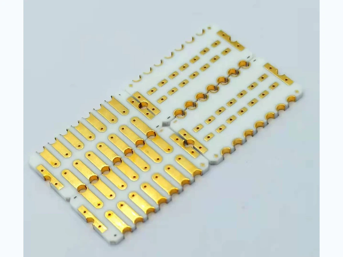
An edge termination carries an electrical connection from a ceramic face toward or around an edge. Its function depends on more than the top-view pad size. Sidewall condition, corner shape, metallization continuity, solder access and the direction of the attached load determine whether the connection can be assembled and inspected reliably. Define the termination as a three-dimensional interface with separate mechanical and electrical requirements. A top-face photograph or a nominal pad dimension alone cannot establish the coverage or performance of the hidden edge region.
Key design decisions
- Specify whether the connection ends at the edge, covers a sidewall, or continues onto the opposite face.
- Define the active contact region separately from the metallization transition around a corner.
- Choose inspection and test access that can reveal a discontinuity at the edge without relying on solder to bridge it.
Distinguish the intended edge construction
An edge-adjacent pad, a castellated feature and a continuous wraparound termination are different constructions. They require different drawings and may use different metallization sequences. Show the relevant faces and identify where continuity is required. If only the front-face pattern is available, do not infer the unseen sidewall coverage from its proximity to the outline.
Describe the purpose of the connection. A spring contact sliding across a sidewall has different finish and wear questions from a soldered wire attached to a top pad. A solder fillet that reaches the edge does not prove there is a controlled conductive path around the ceramic corner. Define the finished interface that the assembly will actually use.
Treat corner shape and edge damage as interface variables
The local edge profile influences how a deposited material transitions from one face to another. A sharp corner, a rounded edge and a chipped sidewall present different surfaces. Specify the intended edge preparation and where its dimensions are assessed. Keep permissible cosmetic chips separate from damage that intrudes into the active termination region.
Inspect edge geometry before assigning a metallization defect. A dark gap may be a coverage loss, a shadow from a chip or an actual crack. Use views that expose the transition and a consistent lighting arrangement. If a cross-section is needed, choose a location that addresses the suspect path rather than sectioning an arbitrary attractive area.
Define the electrical path through the transition
Draw the complete current route from the face trace through the termination and into the attached conductor. A narrow neck or a thin corner region may dominate resistance even when the visible pad is large. Resistance measured across the whole circuit cannot isolate this local contribution unless the measurement includes suitable sense points.
A useful coupon separates the face conductor, edge transition and attachment joint. Measure these segments under the same temperature and contact conditions. Compare the transition before soldering and after attachment. If a low result appears only after soldering, the solder may be bypassing an incomplete metallization path. That behavior needs a construction decision rather than an automatic pass based on final continuity.
Write coverage requirements that can be inspected
Coverage should identify the surfaces and the electrically active region, not simply demand a uniform appearance everywhere. A termination drawing can distinguish the required continuous band, the allowable taper away from it and the connection area that must remain free of overglaze. State how a local interruption is evaluated relative to the current path.
Keep glass protection and electrical access coordinated. Overglaze may protect surrounding traces while leaving a defined soldering or contacting window. Its boundary must not reduce the available termination area below the assembly requirement. Evaluate the fired opening, not just the screen artwork.
| Feature | Functional concern | Useful verification |
|---|---|---|
| Corner transition | Local necking or discontinuity | Side view plus isolated electrical path |
| Sidewall band | Usable connection area | Coverage map against the drawing |
| Overglaze opening | Blocked solder or spring-contact access | Finished opening dimensions |
| Ceramic edge | Chipping or crack origin | Controlled edge photographs and damage location |
| Attached lead | Bending and peel load | Load direction and restrained assembly review |
Plan solder access without using excess solder as compensation
The joint needs sufficient wettable area and physical access for the chosen attachment method. Excess solder can hide an irregular edge while increasing joint stiffness or bridging a neighboring conductor. Define the lead approach direction and the volume envelope for the final fillet. The solder alloy, flux and thermal exposure must be compatible with the chosen termination material.
Inspect the termination before assembly so the solder does not conceal the original condition. After attachment, look for the actual wetting boundary and any ceramic damage near the joint. If rework is permitted, record cumulative heating and mechanical handling. Repeated attachment is a separate exposure, not a return to an unused termination.
Keep cable and contact forces out of the fragile corner
A connection near an edge creates a lever arm when a wire is pulled or bent. The relevant load includes assembly handling and cable movement, not only steady operation. Provide restraint close enough to prevent the joint from carrying the full cable moment, while avoiding a clamp that presses directly on unsupported ceramic.
For a spring contact, define normal force direction, contact travel and the region through which the contact moves during insertion. A contact that starts on the corner and then slides onto a flat face can load the metallization transition differently from a contact that remains on one surface. Describe that sequence in the interface drawing.
Use tests that distinguish continuity from joint strength
Electrical continuity and mechanical attachment strength answer different questions. A termination can conduct before a crack opens under load, while a strong-looking solder fillet can span a locally weak metallization region. Define separate electrical measurements and mechanical loading configurations, with the failure location recorded in each case.
Choose a force direction representative of the attachment. Pulling perpendicular to a face emphasizes peel behavior; pulling along a lead emphasizes another load path. Document the fixture support because a test that bends the ceramic may measure substrate fracture rather than termination adhesion. Compare failure locations and surfaces before interpreting a numerical force as a material property.
Resolve the first failing segment
When an edge connection becomes intermittent, repeat the measurement with the cable immobilized and then with controlled movement. Compare the face trace, corner transition and external joint independently where access permits. Observe whether the fault follows contact pressure, temperature or displacement. Do not increase test current merely to force a marginal path to read as continuous.
The corrective action should address the failed segment: edge preparation, coverage, protected-window geometry, attachment process or strain relief. Replacing the entire material stack before locating the fault makes later comparisons difficult. Keep pre-assembly views, final joint views and the measurement path together so the next design iteration can test a specific change.
Provide the edge-interface definition
Submit the construction and attachment details needed to assess the full connection around the ceramic boundary.
- Drawing views of every electrically active face, with required sidewall coverage and continuity paths identified.
- Ceramic edge profile, permitted damage regions, thickness and any preparation or singulation information.
- Connection type, lead or spring-contact geometry, load direction, restraint and assembly thermal history.
- Overglaze openings, solder or contact requirements, inspection access and the intended electrical and mechanical tests.
The drawing-upload form loads as you reach this section.