
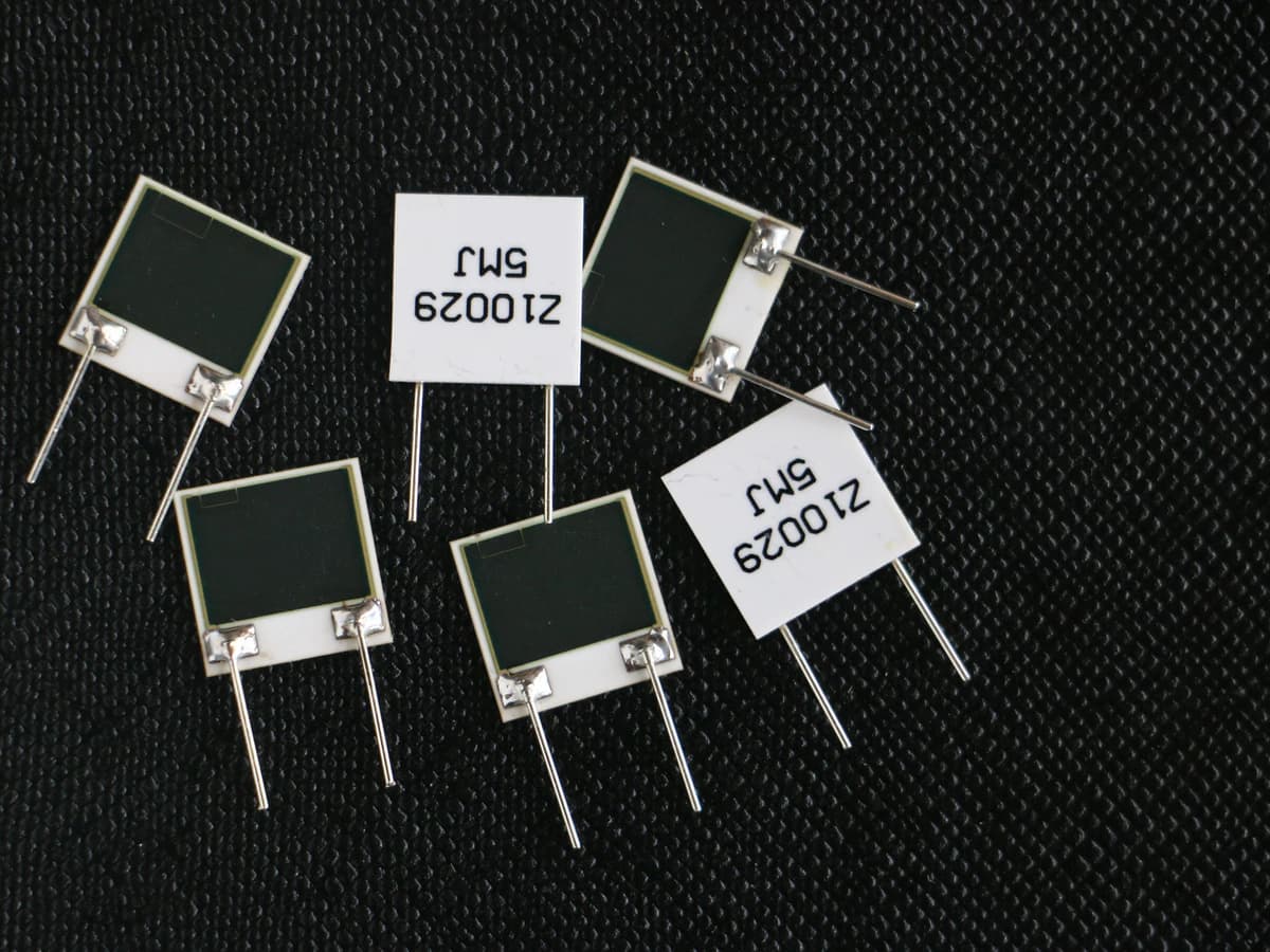
Overview
A solder pad on a thick film ceramic circuit is a material and assembly interface, not only a copper-footprint exercise. Pad behavior depends on the fired conductor and any finish, solder alloy and flux, component or lead, pad geometry, ceramic support, thermal profile, cleaning, environmental exposure, and strain transferred by the assembly. The design should prevent leaching, weak adhesion, cracking, current crowding, contamination, and unreviewed mechanical load through a controlled joint stack and validation plan.
Failure controls
These are review prompts, not evidence that every risk applies or that every test is available.
- A
Choosing pad geometry from an FR4 land pattern without reviewing the fired conductor and ceramic support
- B
Leaching, dewetting, weak adhesion, or interface damage from an incompatible alloy, finish, flux, or thermal cycle
- C
Cracking or chipping the ceramic through stiff leads, edge proximity, fixturing, connector load, or thermal mismatch
- D
Concentrating current or heat in a narrow conductor neck, pad edge, or poorly supported transition
- E
Trapping ionic or chemical residue under protection, components, or inaccessible cleaning regions
- F
Qualifying an isolated joint while the final enclosure, harness, mounting, vibration, or rework creates a different load
Controlled model
Solder-interface evidence decision record
Pad release requires several distinct evidence layers. A surface-wettability result does not prove assembly-process success, a workmanship image does not prove pad adhesion, and a supplier paste result does not qualify a different fired stack.
Decision comparison
| Decision | Route A | Route B | Verification |
|---|---|---|---|
| Surface readiness versus assembly success | A solderability or wetting test evaluates the selected processed surface under a defined conditioning, alloy, flux, temperature, dwell, and evaluation method. | A production-intent assembly trial evaluates the real solder volume, component or lead, heating method, fixture, cleaning, support, and rework sequence. | Record both methods and their limits separately; do not use a surface test as proof that the complete assembly process is qualified. |
| Process requirements versus workmanship acceptance | The contractually selected soldering-process requirements control materials, preparation, equipment, profile, handling, cleaning, and process evidence. | The contractually selected post-assembly acceptance criteria classify observable joint and assembly conditions. | Name the applicable document revision, product class or project criteria, inspection views, sampling, and order of precedence. |
| Named metallization route | One fired conductor and finish stack is reviewed with its compatible alloy, flux, thermal history, protection overlap, storage, and cleaning. | Any alternate conductor, finish, alloy, or protection route is treated as a new interface stack rather than an equivalent substitution. | Use named material evidence within scope and verify wetting, leaching, residues, conductor condition, electrical function, and adhesion on the actual processed stack. |
| Pad geometry and ceramic support | A supported pad keeps the termination load, conductor neck, fillet, edge distance, hole distance, and protection boundary inside the released assembly geometry. | An edge-adjacent, unsupported, stiff-lead, connector-loaded, or reworked pad has a different strain and cracking risk even at the same nominal dimensions. | Inspect the ceramic and joint, then apply drawing-defined pull or shear, electrical, thermal-cycle, vibration, or assembly-level tests with the real support. |
- A conventional FR4 land pattern is not a released thick-film ceramic pad design without metallization, support, and assembly review.
- Record profile temperature in °C, time in s, mechanical force in N, and electrical resistance in Ω or mΩ; values remain drawing- and test-plan-defined.
Solder-interface design review
The order makes assumptions and ownership visible before a result is promoted to a requirement.
- 01
Define the complete joint stack
Identify substrate, fired conductor, pad finish if any, solder alloy, flux, component termination or lead, protective layers, cleaning, rework, and the evidence scope for every interface.
- 02
Translate electrical and mechanical loads
Record current, voltage, heat sources, lead stiffness, connector or wire load, board support, vibration, thermal expansion, mounting, and service handling that can act on the pad or ceramic.
- 03
Lay out pad and protection boundaries
Set pad shape, conductor neck, overlap, spacing, edge and hole clearance, solder and overglaze keep-outs, wetting direction, inspection access, and strain-relief features from the actual assembly geometry.
- 04
Release the soldering process window
Control paste or solder volume, flux, preheat, peak and time history, atmosphere, fixturing, cleaning, repeat cycles, rework limit, and handling without borrowing a generic profile as a product specification.
- 05
Qualify the joint and ceramic interface
Inspect wetting, coverage, residues, conductor condition, cracks, and alignment; measure electrical function and apply project-relevant mechanical, thermal, vibration, or environmental tests to the production-intent assembly.
Engineering review matrix
Each row links a design variable to evidence that can support a drawing or release decision.
| Variable | Control question | Verification route |
|---|---|---|
| Pad metallization and finish | Identify the fired conductor, thickness or processed state where known, finish or plating, refires, protection overlap, solderability basis, and storage condition. | Review named material evidence and inspect the actual processed pad before and after the released solder cycle. |
| Solder, flux, and cleaning system | Define alloy, form, flux chemistry, volume, atmosphere, residues, cleaning process, compatibility, and rework materials. | Use supplier process information within scope and verify wetting, residues, corrosion risk, and electrical cleanliness on the real stack. |
| Pad and conductor geometry | Set pad dimensions from the actual termination, solder fillet intent, conductor neck, overlap, current path, mask or overglaze boundary, neighboring features, and inspection access. | Measure the released geometry and inspect solder coverage and conductor condition at the pad edges and neck-down. |
| Ceramic edge and support | Define pad distance from edges, holes, score lines, unsupported regions, clamps, fixtures, and load paths through the brittle substrate. | Inspect for chips and cracks before and after assembly and test the product in its production-intent support condition. |
| Thermal process history | Record preheat, peak, time, cooling, local heat input, number of cycles, prior firings, component thermal mass, and rework exposure. | Capture the workpiece profile where needed and compare joint, conductor, and substrate condition across permitted cycles. |
| Mechanical strain and retention | Account for termination mass and stiffness, wire or connector loads, pull direction, vibration, shock, housing expansion, handling, and strain relief. | Apply agreed pull, shear, vibration, thermal-cycle, or assembly-level loading with the real support and failure criteria. |
| Electrical and thermal loading | Define current, voltage, duty, local resistance, nearby heat sources, temperature range, and allowed voltage drop or heat concentration. | Measure joint resistance or functional output and local temperature under representative operating conditions. |
| Inspection and acceptance | Agree visual views, wetting or coverage criteria, void method if relevant, residues, cracks, continuity, adhesion or mechanical checks, sampling, and disposition. | Use a drawing-linked inspection plan and retain representative records and approved exceptions. |
Reference boundary
Public method sources
These sources support the engineering method and terminology used in this technical guide. They do not establish a ThickFilmPCB material list, capability limit, customer result, certification, or finished-product specification.
- 01IPC J-STD-003D — Solderability tests for printed boards
Supports wettability and solderability test-method boundaries for printed-board conductors and lands only; the standard explicitly does not determine pad-design impact and does not establish ceramic-pad or ChipSimple capability.
- 02IPC official release overview — roles of J-STD-001J and IPC-A-610J
Provides a high-level official distinction between soldering process and material requirements in J-STD-001J and post-assembly acceptance in IPC-A-610J only. Detailed criteria require the applicable licensed standards and contractual selection; this overview does not qualify a thick-film ceramic joint.
- 03Heraeus — C2130B silver/palladium conductor technical data sheet
Supports reviewing metallization, fired thickness, solder system, leach resistance, adhesion, and process conditions together for one named paste only; its test values are not transferable to another stack or claimable as ChipSimple performance.
Inputs for a practical review
Unknown values may be labelled unknown. The review should convert uncertainty into an explicit decision or validation task.
Send Drawings- 01
Ceramic and printed-layer drawing with pad, conductor, protection, edge, holes, score lines, datums, and support
- 02
Fired conductor and finish information, component or lead drawing, termination material, and storage or handling limits
- 03
Solder alloy and form, flux, volume, atmosphere, thermal profile, cleaning, inspection, and rework process
- 04
Current, voltage, duty, local heat sources, operating and assembly temperatures, and allowed electrical change
- 05
Lead, wire, connector, fixture, mounting, housing, pull, vibration, shock, and thermal-expansion loads
- 06
Required visual, dimensional, electrical, mechanical, environmental, sampling, and report criteria
- 07
Prototype quantity, production assembly sequence, acceptance owner, failure analysis, and change-control plan