
On this page
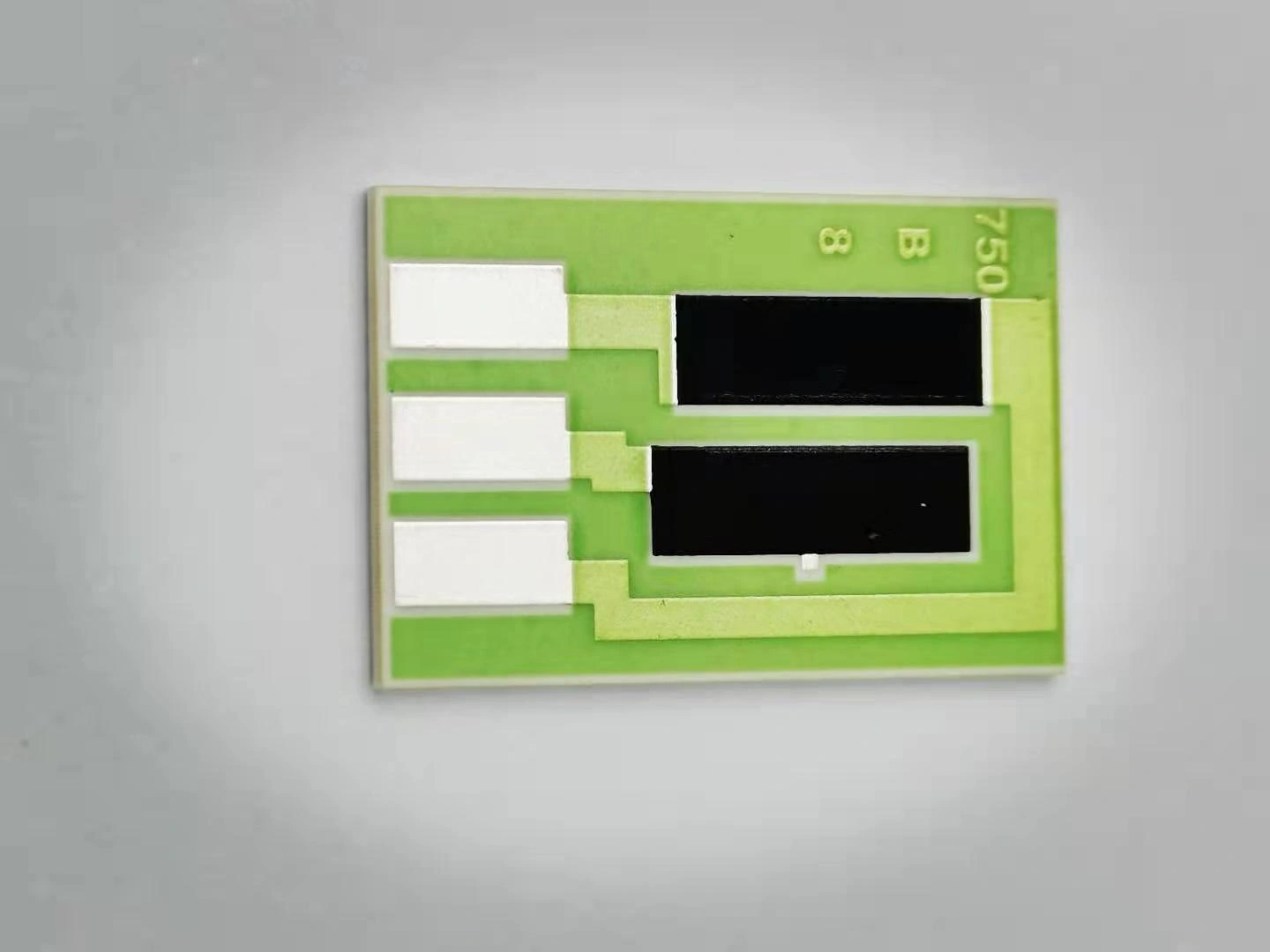
A coplanar comb and a buried conductor overlap can both produce an insulation-resistance reading, but they do not challenge the same physical path. The comb exposes a long neighboring-electrode boundary to the surrounding surface condition. The overlap directs the question toward the separating dielectric stack and its edges. Select the test vehicle from the location of the suspected path before specifying an instrument reading or comparing materials.
Key design decisions
- Draw the current path and identify the surface or buried layer being challenged.
- Preserve material and processing history when transferring a test vehicle to ceramic.
- Do not convert contaminated comb resistance into an assumed universal sheet resistivity.
- Use separate structures when surface exposure and buried-layer integrity are independent concerns.
1. Draw the path the coupon must retain
Mark the driven electrode, measured electrode, surrounding conductors and any guard on a section and plan view. Identify whether current is meant to travel across exposed ceramic, across an overglaze surface, along an interface or through a fired dielectric. Record other possible routes that the fixture might include or deliberately exclude.
A coupon that is easy to probe may omit the product feature that matters. For example, a large flat overlap does not reproduce the dielectric step at a lower conductor edge. A bare ceramic comb does not reproduce residue trapped beneath a later coating. Make the retained and omitted features explicit before using the coupon to answer a product question.
2. Use a comb for a neighboring-surface question
An interdigitated pattern places many opposing electrode edges within a small area. It can be useful when a process comparison concerns residue, moisture and degradation between adjacent exposed features. The path includes the actual electrode material and the surface between it; neither should be replaced casually when transferring the design.
A standardized printed-board comb and a custom fired ceramic comb are different test vehicles. Changing the substrate, conductor, gap or preparation history requires a bounded comparison and a declared method, rather than an automatic claim that the modified vehicle retains a standard classification. Keep the material-specific exposure conditions with the relevant qualification requirement.
3. Use an overlap to retain the buried stack
A lower electrode, dielectric and upper electrode can expose a through-layer path that a coplanar pattern never challenges. Match the material sequence, actual separating thickness and conductor topography to the question. The top electrode must not create an unintended short at the edge of the lower electrode or through an uncovered region.
Decide whether edge leakage belongs in the measured result. An unguarded overlap can include edge and bulk contributions together. A guarded material arrangement can suppress an unwanted surface route, but that may remove a route that exists in the final circuit. A cleaner-looking bulk result is not automatically a more representative assembled-circuit result.
4. Calculate the geometric change without redefining the material
Consider a deliberately ideal comparison: an initially uniform, ohmic dielectric has 20 µm thickness, 4 mm² effective area and a measured resistance of 5 GΩ. Using R = ρt/A gives an apparent bulk resistivity of 1 × 10⁹ Ω·m, equivalent to 1 × 10¹¹ Ω·cm. Doubling the area to 8 mm² would halve resistance to 2.5 GΩ if the same uniform model remains valid.
Those predictions fail if edge leakage dominates, the thickness distribution changes or a local defect controls the path. Doubling area also increases the amount of material sampled; it does not prove an unchanged probability of encountering a defect. Use geometry scaling as a consistency check supported by additional specimens, not as a substitute for investigating a changed current path.
5. Do not assign sheet resistivity to a patchy contaminated comb
For an ideal uniform conducting surface, a geometric model can relate resistance to path width and length. A contaminated comb need not behave as that uniform surface. Residue may accumulate near one finger, leave isolated clean regions or change during bias. One local path can dominate the measured current even when most of the pattern looks unchanged.
A simple parallel-path example shows the problem. Ten equal independent paths of 100 GΩ would combine to 10 GΩ. If one path changes to 1 GΩ while the other nine remain at 100 GΩ, the total becomes 1/(1/1 + 9/100), or approximately 0.917 GΩ. The result is dominated by the changed path; multiplying by a drawing-based factor does not recover a universal property of the entire surface.
6. Select the structure from the decision, not the available footprint
More than one structure may be needed on a process coupon, but each must retain its own identity and result. Separate patterns are not interchangeable readings of one insulation-quality number.
| Decision to support | Feature to retain | What the result cannot establish alone |
|---|---|---|
| Residue-related conduction between exposed traces | Coplanar electrodes with representative surface and gap | Integrity through a buried fired dielectric |
| Leakage through a flat dielectric region | Defined opposing-electrode area and separating thickness | Adequate coverage over a conductor step |
| Isolation near a real crossover edge | Representative step, overlap and exposed perimeter | A geometry-independent bulk material constant |
| Material volume-resistivity comparison | Appropriate electrode geometry and controlled surface-current exclusion | Total leakage of an unguarded assembly |
| Effect of overglaze on a neighboring surface path | Actual glaze boundary, exposed openings and treatment history | Protection provided by a different glaze geometry |
| Comparison between two comb layouts | Mapped geometry, matched history and local observations | A universal normalization for nonuniform residue |
7. Keep the comparison tied to the same processing population
Allocate the chosen structures across the positions and process runs relevant to the investigation. A coupon at the easiest-to-clean edge of a panel may not represent a dense interior product region. Record the material lot, surface preparation, firing sequence and subsequent handling for each structure, including any attachment operation used to connect test leads.
When a cleaning or coating change is evaluated, use the same starting construction and retain a baseline branch. Avoid giving only the candidate coupon special handling that the product will not receive. Multiple patterns on one substrate provide useful spatial information, but they do not create the same number of independently processed substrates. Report both counts so the comparison remains interpretable.
8. Deliver a coupon drawing with an interpretation boundary
The drawing should identify electrode connections, guard state, critical dimensions, inspected surfaces and the intended measurement interval. Pair it with the permitted environment, electrical stimulus and stopping criteria from the responsible test plan. Use a laboratory arrangement appropriate for the applied voltage, with controlled access and discharge; a coupon layout is not a complete electrical-safety design.
The final conclusion should name the supported path. A successful surface-process comparison can support that surface and history without qualifying every buried dielectric region. A successful overlap result can support that stack without proving resistance to residue across exposed openings. Where both functions are required, keep both results and resolve disagreement through location-specific inspection rather than averaging them into a single pass value.
Send the insulation path and proposed test vehicle
Provide the structure and process decision before choosing a coupon solely from an existing artwork file.
- Product section showing electrode layers, dielectric or glaze boundaries and exposed surfaces
- Proposed comb or overlap artwork with gaps, effective areas and dimensional state
- Material identities and complete print, fire, clean, coat and lead-attachment history
- Whether edge and surface leakage must be included or guarded away
- Required operating or qualification conditions and specimen allocation by panel and run
- Existing time-dependent measurements and location-matched inspection records
The drawing-upload form loads as you reach this section.