
On this page
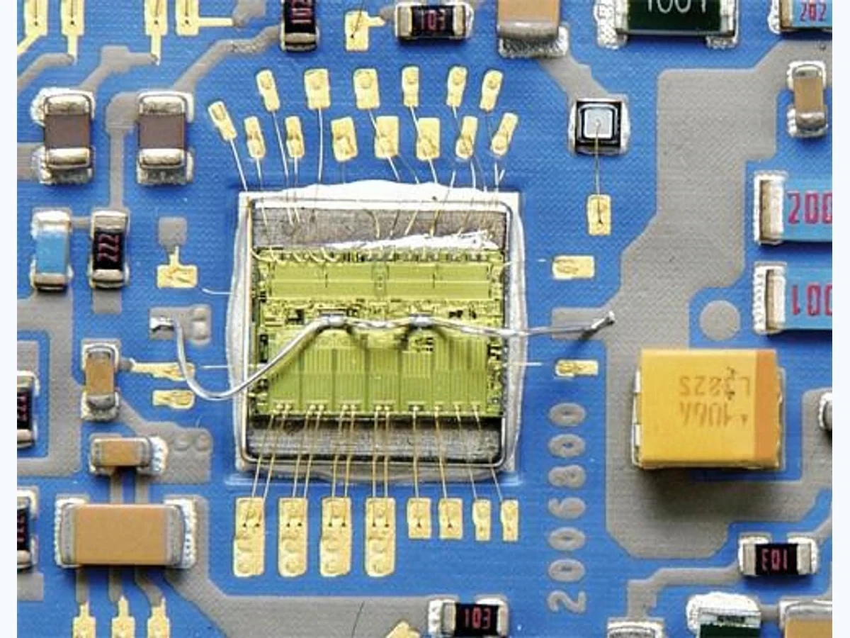
A gold thick film bond pad has two related but separate jobs: it provides a suitable bonding interface and connects that interface electrically to the rest of the circuit. A large shiny pad does not establish bondability, and a successful bond does not by itself establish acceptable current loss through a narrow connecting trace. Review the surface, pad support, conductor route and bonding access as one interface while keeping the acceptance criteria for each function distinct.
Key design decisions
- Specify the intended wire, bonding method and pad surface condition with the conductor material.
- Keep the bond landing area separate from the neck that carries current away from it.
- Evaluate bonding results at the final surface state after all relevant firing, cleaning and handling operations.
Separate the bond landing from the conductor route
Mark the area where the bond tool may land and the path from that area to the next circuit node. The landing region needs adequate size and support for the bonding process. The connecting route needs sufficient electrical and thermal margin for the current it carries. These dimensions should be reviewed independently.
A narrow neck can increase local resistance even when the pad is broad. Conversely, widening the neck does not correct a contaminated or unsuitable bonding surface. Define the current path, bond position and mechanical support so an electrical failure is not addressed only by changing bonding parameters.
Identify the actual processed gold surface
The word gold does not fully define the bonding interface. A thick film conductor includes a processed structure associated with its material formulation and firing sequence. A plated or thin-film gold finish is a different surface and should not be substituted in the technical description.
Record the selected gold-conductor grade and distinguish wet, dried and fired material states before evaluating the bonding interface. Use the selected conductor's bonding compatibility information and do not infer a universal wire-bond specification from color or nominal metal content.
Provide tool access and a supported landing region
The pad must accommodate the intended bond footprint and placement variation without allowing the tool to overlap an unsuitable edge or nearby material. Include the approach envelope, neighboring components and any wire-loop clearance. A pad can be large enough in area but inaccessible because a tall adjacent part blocks the tool.
Check the support beneath the landing area. Local substrate bending or a nearby cavity changes how force is transmitted during bonding. If the circuit is already attached to a package, review the package support state at the bonding operation, not only the final assembled condition.
Calculate the path between the bond and the circuit node
Estimate resistance in the printed route using the relevant fired geometry and electrical data. Include the bond wire and any other series interconnect when evaluating voltage available to a load. Keep wire and pad losses separate so the design change targets the dominant contributor.
At higher current, local heating can alter the joint environment and the nearby circuit. Evaluate duty cycle and cooling rather than treating the gold surface as an unlimited conductor. For a low-current sensing path, stable connection resistance and thermoelectric effects may be more important than total power dissipation.
For a hypothetical connection carrying 0.5 A, a measured combined wire-and-trace resistance of 0.08 Ω gives a 40 mV drop and 20 mW of dissipation. The calculation uses V = IR and P = I²R. It does not establish a current rating, because local temperature depends on where that resistance is concentrated and how heat leaves the wire, pad and substrate. Measure the relevant segments if the permitted voltage drop is close to the calculated result.
Use different checks for bonding and conduction
The inspection record should show which function each result verifies. A visually acceptable bond and a low-resistance path are complementary observations, not interchangeable proof.
| Function | Critical condition | Appropriate evidence |
|---|---|---|
| Bond formation | Wire, surface and process compatibility | Bond evaluation with failure location |
| Landing accuracy | Pad boundary and placement variation | Bond-footprint inspection |
| Mechanical support | Local substrate and package stiffness | Review of support during bonding |
| Electrical conduction | Trace and wire series resistance | Defined-point electrical measurement |
| Thermal behavior | Current and heat-removal path | Loaded temperature and resistance observation |
| Surface preservation | Post-fire handling and cleaning | Traceable final surface condition |
Protect the surface through the full sequence
List every operation after the gold conductor is formed: additional firing, cleaning, handling, attachment and storage. The bondable surface is the state produced by that sequence, not the state immediately after an isolated material trial. Keep contact tools and storage surfaces appropriate to the finish.
If a cleaning operation is changed, evaluate the resulting bond interface rather than assuming cleaner appearance means better bonding. Residue, surface damage or incompatible chemistry can affect the next operation. Preserve the same wire and bonding setup during the comparison so the cleaning effect can be distinguished.
Interpret the failure surface before adjusting the process
A failed bond evaluation can involve the wire, the wire-to-metal interface, the metallization or the ceramic beneath it. Record where separation occurred. A numerical pull or shear result without a failure location can hide a change from one limiting mechanism to another.
If electrical resistance changes while mechanical strength remains similar, investigate the conductor neck and the measurement contacts as well as the bond itself. If metallization lifts, increasing bonding energy may worsen the problem. The corrective action should follow the observed interface behavior, with the material and surface history kept visible.
Keep the sequence of destructive and nondestructive checks deliberate. Measure the electrical path and photograph the bond before a pull or shear operation changes it. After the mechanical test, preserve the remaining wire and pad surfaces in their original orientation. If a section is prepared, choose its location from the observed failure and record the preparation method. These steps make the evidence useful for separating poor bond formation from weak metallization or substrate damage.
Deliver the bonding interface as a complete requirement
Include the conductor grade, finished pad dimensions, wire or ribbon specification, bond method and permitted landing region. State the process stage at which the pad is inspected and bonded. Add nearby topography and package constraints that affect access.
For a circuit review, provide operating current, voltage-drop sensitivity and the required environmental exposure. This allows the bonding and electrical requirements to be assessed together. Avoid a general instruction to use gold for reliability; define the actual interface and the evidence needed for its intended function.
Send the gold bond-pad requirements
Provide the bonding interface and the electrical route connected to it.
- Conductor grade, pad and neck artwork, fired state and all later thermal or cleaning operations.
- Wire or ribbon material, bonding method, footprint, tool approach and package support.
- Current waveform, voltage-drop allowance, temperature environment and sensitive measurement requirements.
- Bond-test failure locations, footprint images and defined-point electrical measurements.
The drawing-upload form loads as you reach this section.