
Overview
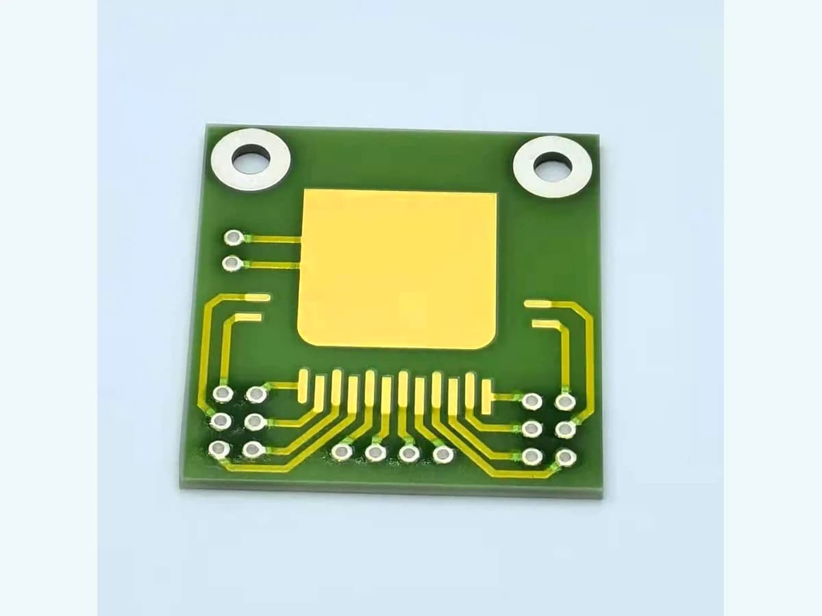
Gold conductor paste is selected for a specific processed interface, not because a circuit is premium, high temperature, corrosion resistant, or wire bondable in the abstract. Supplier gold systems differ in substrate scope, inorganic or polymer binder, compatible dielectrics, screen and thickness, drying, firing or curing, atmosphere, refires, resistivity, fine-line behavior, solder or wire-bond intent, adhesion test, storage, and restrictions. A fired gold conductor designed for alumina or a low-temperature ceramic may not suit AlN, an organic film, another firing profile, soldering, brazing, thick aluminum wire, or direct environmental exposure. Even a documented wire-bondable paste requires a complete pad and bond process: fired surface, contamination, pad geometry, substrate support, wire metallurgy and diameter, tool, energy, force, temperature, loop, cleaning, pull or shear method, and post-bond conditioning. This guide keeps material selection, conductor geometry, process history, joining, and validation connected. It does not identify the photographed gold-colored surface as a named paste and does not claim any ThickFilmPCB gold purity, resistance, line, bond, adhesion, corrosion, temperature, or reliability capability.
Engineering review matrix
Each row links a design variable to evidence that can support a drawing or release decision.
| Variable | Control question | Verification route |
|---|---|---|
| Gold material identity | Record supplier, product code, fired ceramic or polymer route, composition description, lot, shelf state, storage, conditioning, thinner, and substitution prohibition. | Use current supplier TDS and receiving records; never infer chemistry from color or a prior product photo. |
| Substrate and companion system | Specify grade, surface, conductor and dielectric compatibility, resistor, overglaze, attach, finish, wire or solder, coating, layer order, and refires. | Qualify the full processed stack and preserve material and traveler traceability. |
| Print and final geometry | Set screen, emulsion, artwork, wet and final thickness, line width and edge, overlaps, turns, necks, pad size, spacing, and registration. | Measure production-intent features and correlate them with resistance, current distribution, surface, and joint results. |
| Firing or cure history | Define atmosphere, ventilation, equipment load, time-temperature profile, peak, dwell, cooling, refires or repeat cures, and later assembly heat. | Retain traceable profiles and witness measurements after every relevant thermal stage. |
| Electrical loading | State continuous and transient current, voltage, pulse, duty, acceptable drop, local heating, bias, fault current, and diagnostic conditions. | Record path resistance, voltage, current, and mapped temperature in the real stack through nominal, tolerance, and fault states. |
| Wire-bond or solder process | Define wire or solder metallurgy, dimensions, tool, energy or thermal profile, force, dwell, atmosphere, flux, cleaning, rework, loop or joint geometry, and strain relief. | Inspect and test production joints, classify failure mode, and condition them through representative assembly and use exposure. |
| Surface cleanliness and protection | Control handling, time from firing to joint, storage, cleaning media, residues, probe marks, overglaze or coating edges, contamination, and repair. | Use defined surface or cleanliness checks and compare joint and electrical response before and after controlled exposure. |
| Environment and evidence | Specify thermal cycling, humidity, condensation, fluids, corrosives, bias, vibration, shock, storage, sampling, uncertainty, records, and change triggers. | Run the drawing-linked validation plan and retain lot, process, test, failure, reviewer, and release evidence. |
Controlled model
Gold path and joining-interface model
Use the supplier's stated fired or cured thickness and test construction when translating sheet resistance into a geometry estimate. Treat the conductor body, transitions, pad, bond or solder joint, substrate interface, and protection as separate failure opportunities.
R_path ≈ R□(L/W) + ΣR_transition + ΣR_jointFirst-order total path resistance including printed body, geometric transitions, and electrical joints.
- Units
- All resistance terms in Ω; R□ in Ω/□
- Use boundary
- Assumes the applicable sheet-resistance convention and approximately uniform film. Printed thickness, pores, corners, overlaps, refires, bonds, and contacts require measured correlation.
V_drop = IR_path; P = I²R_pathVoltage loss and Joule heating along the complete current path at a stated current.
- Units
- V in V; P in W; I in A; R in Ω
- Use boundary
- Does not define allowable current, pad temperature, or life. Include pulse, duty, local geometry, heat path, interface resistance, wire, connector, ambient, and faults.
J_nom = I/(Wt)Nominal current density in a uniform printed cross-section used for preliminary comparison.
- Units
- A/mm² or A/m²
- Use boundary
- Not a local peak. Current crowds at necks, corners, vias, bond footprints, probe marks, cracks, porosity, and conductor transitions; use measured geometry and detailed analysis when needed.
σ_app = F_test/A_refApparent normalized mechanical test stress using a defined force and reference pad or bonded area.
- Units
- N/mm² when F is N and A is mm²
- Use boundary
- Wire pull, ball shear, stud pull, peel, and substrate-interface tests have different force paths and failure modes. Do not compare normalized values without the same method and construction.
Decision comparison
| Decision | Route A | Route B | Verification |
|---|---|---|---|
| Fired gold versus polymer gold composition | A fired system uses a supplier-defined ceramic, screen, drying, furnace atmosphere and profile, fired thickness, compatible layers, and refire history. | A polymer gold system uses a formulation-specific organic substrate, solvent interaction, drying or cure, thickness, adhesion, flexibility, and assembly-temperature boundary. | Keep process routes, materials, fixtures, evidence, and terminology separate; qualify the exact system rather than transferring gold-metal assumptions. |
| Wire-bondable versus solderable conductor | Wire bonding depends on fired surface and pad metallurgy, contamination, support, wire, tool, force, energy, temperature, loop, and bond test. | Soldering depends on solder and flux, wetting, leaching or dissolution, dwell, reflow cycles, cleaning, intermetallics, pad geometry, joint strain, and inspection. | Use a paste explicitly scoped for the intended joint and validate that production-intent interface; do not treat the two labels as synonyms. |
| Fine line versus robust pad build | A fine routed line prioritizes print definition, thickness uniformity, resistance, registration, conductor edges, isolation, and local current density. | A joining pad prioritizes surface condition, area, support, repeated bonding or solder exposure if applicable, adhesion, load path, cleaning, and inspection access. | Include both geometry families on qualification coupons and evaluate them after the complete layer and assembly sequence. |
- A gold-colored image can result from several metallization or finish routes; visual appearance cannot identify chemistry, thickness, purity, or process.
- A supplier's 850°C value, where present, is a peak firing-process condition for the named material system and never a finished circuit operating-temperature rating.
Failure controls
These are review prompts, not evidence that every risk applies or that every test is available.
- A
Choosing gold from color, prestige, or corrosion assumptions without matching exact supplier system, substrate, companion layers, process, and joint
- B
Calling a conductor wire bondable or solderable without qualifying pad surface, wire or solder, tool, parameters, support, cleaning, loads, and failure method
- C
Using sheet resistance from one thickness and geometry while printed edges, pores, necks, refires, transitions, and joints dominate the production path
- D
Combining fired ceramic gold and polymer gold evidence or describing a firing-process peak as finished operating temperature
- E
Allowing contamination, probing, storage, dielectric bleed, overglaze edges, rework, or repeated bonding to change the pad outside inspection
- F
Publishing gold purity, bond strength, resistance, line definition, adhesion, corrosion, temperature, or reliability without controlled company evidence
Gold conductor selection workflow
The order makes assumptions and ownership visible before a result is promoted to a requirement.
- 01
Define conductor and joint functions
Separate routed interconnect, die-attach area, wire-bond pad, solder pad, contact, electrode, resistor termination, crossover, or decorative finish. State current, voltage, loss, geometry, assembly, environment, inspection, and failure consequence for each.
- 02
Freeze substrate and stack
Name alumina, AlN, LTCC, organic film, or other exact substrate product and surface; conductor, resistor, dielectric, overglaze, finish, attach, wire, solder, coating, and layer sequence. Do not assume gold makes incompatible layers compatible.
- 03
Review named supplier systems
Compare product code, intended use, substrate, printing, thickness, drying, firing or cure, atmosphere, refires, resistivity, line definition, compatible dielectrics, adhesion, solder or wire-bond scope, storage, safety, test geometry, and disclaimers.
- 04
Design electrical and pad geometry
Calculate a preliminary path, then include fired or cured width and thickness, turns, necks, overlaps, pad size, tool access, edge and dielectric clearance, substrate support, current crowding, thermal path, protection, and inspection datums.
- 05
Process diagnostic coupons
Use traceable lots and production-intent screen, print, dry, furnace or cure, atmosphere, refires, other functional layers, trim, cleaning, pad handling, bonding or soldering, rework, coating, and storage. Keep unbonded controls for separation.
- 06
Test interfaces and function
Measure printed geometry, thickness, resistance, visual and surface condition, adhesion and failure plane, joint pull, shear, peel or other selected method, electrical continuity, isolation, local heating, and post-process change with uncertainty stated.
- 07
Validate exposure and control change
Apply thermal, humidity, bias, corrosion, chemical, vibration, shock, load, storage, and life sequences required by the real system. Link the accepted gold stack and joint process to the drawing and reopen after a controlled input changes.
Reference boundary
Public method sources
These sources support the engineering method and terminology used in this technical guide. They do not establish a ThickFilmPCB material list, capability limit, customer result, certification, or finished-product specification.
- 01Heraeus C5729 Gold Conductor technical data sheet
Supports one named fired gold paste's printing, drying, 850°C firing-process condition, thickness, compatible dielectrics, storage, and stated Al or Au wire-bond intent; it supplies no finished operating rating or ThickFilmPCB capability.
- 02DuPont 5771 Gold Conductor technical data sheet
Supports tying one gold conductor's line, thickness, resistance, alumina test substrate, drying, firing, refires, compatible dielectric, and bond setup together; laboratory results cannot be transferred to another process.
- 03Heraeus C5819 Gold Conductor technical data sheet
Provides a second named supplier system with its own substrate, process, geometry, properties, bond conditions, and limitations, supporting comparison by complete TDS rather than generic gold-metal assumptions.
Inputs for a practical review
Unknown values may be labelled unknown. The review should convert uncertainty into an explicit decision or validation task.
Send Drawings- 01
Circuit and assembly drawings marking gold conductor functions, lines, pads, joints, current paths, voltage, pulse, duty, spacing, protection, and inspection zones
- 02
Exact substrate product and surface, conductor, resistor, dielectric, overglaze, attach, wire, solder, flux, adhesive, coating, and compatible-stack requirements
- 03
Candidate gold material codes, fired or polymer route, supplier documentation, storage, shelf, lot, thinner, allowed or prohibited substitutions, and compliance needs
- 04
Print, dry, firing or cure atmosphere and profile, final thickness, refires, trim, cleaning, probing, bonding or soldering, rework, assembly heat, and storage
- 05
Wire or solder metallurgy and dimensions, bond or reflow tool and parameters, pad support, joint geometry, pull, shear, peel, wetting, continuity, and failure criteria
- 06
Temperature, humidity, condensation, bias, fluids, corrosives, vibration, shock, mechanical load, storage, cycling, and fault conditions
- 07
Prototype and coupon quantity, lots, sampling, measurement uncertainty, conditioning, acceptance rule, traceability, report fields, reviewers, and change control