
On this page
Miniaturizing a thick film ceramic circuit changes the relationship between functional geometry and process variation. A small absolute edge displacement consumes a larger fraction of a narrow conductor, resistor or contact window. At the same time, probes, assembly tools and inspection systems still need physical access. A compact layout should therefore be reviewed for measurable functional margins, not only for whether all shapes fit inside the outline. Preserve the features that establish electrical performance and verification before reducing decorative spacing or redundant area.
Key design decisions
- Identify which dimensions directly control resistance, insulation, connection overlap and mechanical fit.
- Reserve inspection and test access before shrinking the remaining circuit area.
- Separate minimum nominal feature size from the smallest finished feature that remains functional at its tolerance limits.
Rank features by the consequence of variation
A narrow current-carrying trace, a resistor width and a mounting clearance do not respond to variation in the same way. A small change in a resistor width can directly affect resistance, while the same change in a large landing pad may have little effect until a contact-overlap limit is crossed. Classify features by function before applying one common dimensional rule.
Identify the failure condition for each critical feature. Examples include a lost electrical connection, insufficient protected dielectric overlap, a resistor outside its adjustment range or a probe that cannot contact the intended pad. This produces a practical margin map rather than a drawing covered with equally tight tolerances.
Look at relative error as dimensions become smaller
For a rectangular resistor, the simple sheet-resistance model makes resistance proportional to length and inversely proportional to width. The same absolute width variation has a larger fractional effect when the nominal width is reduced. The model does not include end effects or local thickness variation, but it exposes why aggressive scaling can consume the tolerance budget.
As a hypothetical geometric comparison, a 0.02 mm width change is two percent of a 1 mm feature and ten percent of a 0.2 mm feature. These are arithmetic examples, not a statement of printing capability. Use measured process variation for the intended material and pattern to decide whether the compact feature has sufficient margin.
ΔR/R ≈ ΔRs/Rs + ΔL/L − ΔW/W
- R: nominal rectangular film resistance
- Rs: sheet resistance under the defined processing condition
- L and W: effective resistor length and width
- Δ terms: small deviations from the nominal values
First-order sensitivity for a uniform rectangular resistor. Correlation, end effects and nonuniform film thickness are not included.
Review the smallest remaining overlap after registration
Small layouts often depend on several layers meeting inside a narrow region. A via capture pad, dielectric crossover and overglaze opening each have their own positional and edge variation. Inspect the remaining functional overlap after those contributions are combined, rather than checking nominal alignment alone.
A protective layer that is visually centered can still restrict a small solder or probe pad. Include the final fired opening and the assembly placement allowance in the same overlay. Where margin is inadequate, enlarging one landing feature may be more effective than reducing every process tolerance on the drawing.
Reserve physical access for the operations that matter
A circuit that cannot be tested or assembled without touching neighboring features may be compact only on the screen. Tool access should be represented as a physical envelope, including the approach direction and any permitted movement.
| Operation | Space to preserve | What happens if it is omitted |
|---|---|---|
| Electrical probing | Pad area and probe approach clearance | Unstable contact or unintended neighboring contact |
| Laser adjustment | Reachable trim region and protected neighbors | Insufficient adjustment or damage risk |
| Component placement | Tool envelope and placement allowance | Collision or uncertain seating |
| Wire bonding | Bond pad and tool access | Bonding interference despite adequate pad metal |
| Optical inspection | Visible boundary and identifiable datum | A dimension exists but cannot be measured reliably |
| Singulation | Support and edge keepout | Damage during separation rather than electrical fabrication |
Define what the inspection system must distinguish
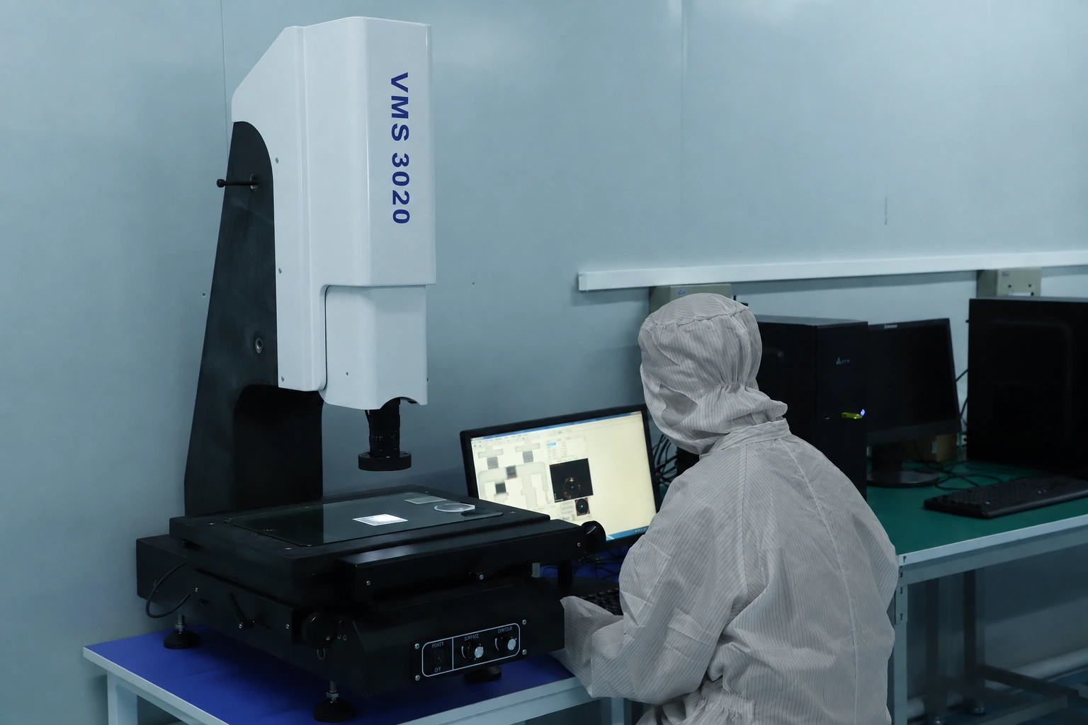
The inspection task is not simply to display a magnified image. It must identify the relevant edge, separate neighboring materials and measure the feature against its acceptance boundary. A shiny conductor beside a translucent glaze may need a different lighting condition from a bare ceramic hole.
Choose measurement locations that correspond to the functional dimension. The widest visible portion of a resistor does not necessarily represent its effective current-carrying width. If a feature is too small or obscured for the selected method, either change the inspection approach or redesign access. Do not declare an unmeasurable dimension controlled because the nominal artwork is precise.
Keep the material route explicit
Thick film, thin film and other ceramic metallization routes have different process characteristics. A small feature demonstrated with one route does not establish the same result for another. Material suppliers document specific printing and firing conditions, and those conditions must remain associated with the feature data being evaluated.
If miniaturization requires a process change, review electrical properties, bonding compatibility, repair options and thermal history as well as nominal resolution. A narrower line achieved by a different material may change resistance or assembly behavior. The design decision is the complete functional route, not a single minimum line-width comparison.
Use a compact-feature coupon that answers a specific question
A useful evaluation coupon includes the actual narrow feature, neighboring geometry and layer interactions that make the design difficult. An isolated straight line may not represent a dense pattern beside a dielectric step. Include measurement structures that can separate dimensional variation from material variation.
Compare a small set of deliberate geometry changes rather than a large uncontrolled mixture. For example, vary the landing-pad allowance while holding the via and alignment method constant. Record both the achieved dimensions and the functional result. A feature that looks clean but has unstable electrical behavior should not be selected on appearance alone.
Choose where to spend the remaining area
The best compact design may use unequal margins. Preserve larger allowance where errors accumulate or where inspection is difficult, and accept tighter packing where the function is less sensitive. Reducing a noncritical space can create room for a more robust connector pad without increasing the overall outline.
Complete the review with the final assembly state. Components, overglaze and package walls can remove access that existed on the bare circuit. Record which dimensions remain critical after assembly and which are verified earlier in the process. This keeps the compact layout manufacturable and testable rather than merely drawable.
Send the compact-layout constraints
Provide the functional limits and the operations that must fit inside the available area.
- Artwork and mechanical outline with critical resistance, insulation, connection and locating features identified.
- Permitted final dimensions, measured process variation and required electrical adjustment ranges.
- Probe, assembly, bonding and singulation access envelopes in the actual process sequence.
- Package clearances, material route and the inspection method intended for each critical feature.
The drawing-upload form loads as you reach this section.