
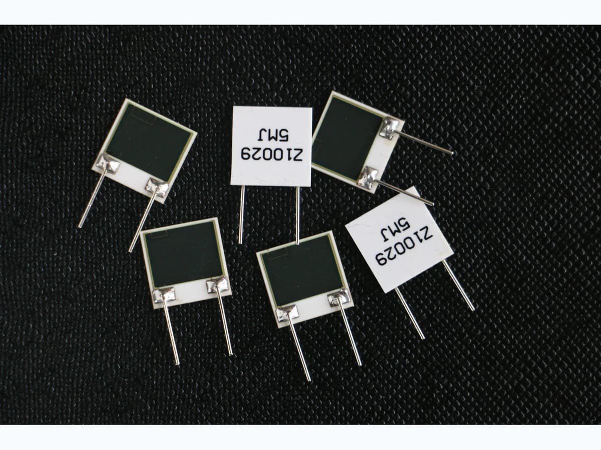
Overview
Thin film and fired thick film resistor networks are different material and patterning routes, not quality grades on one linear scale. this guide compares deposited and patterned thin-film networks with printed-and-fired thick-film networks through absolute value and ratio budgets, TCR and tracking, stability, noise, voltage and power loading, geometry, trimming, protection, assembly, evidence, and project constraints without claiming that either route is universally superior or available.
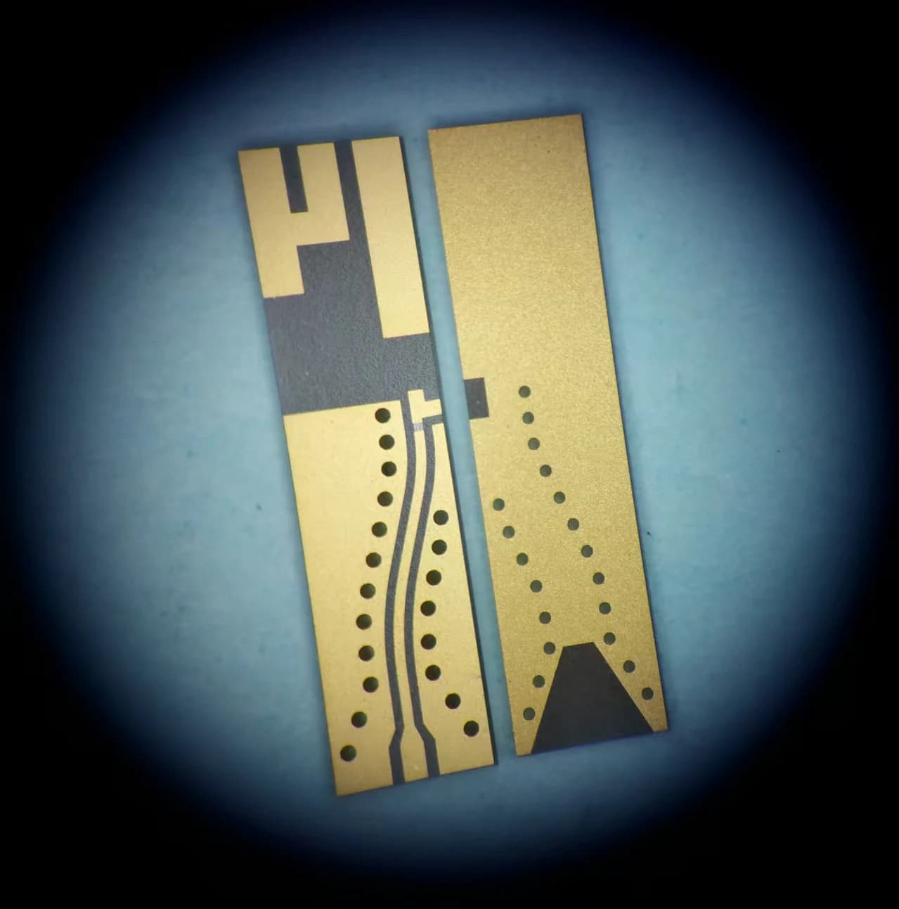
Engineering review matrix
Each row links a design variable to evidence that can support a drawing or release decision.
| Variable | Control question | Verification route |
|---|---|---|
| Process and resistor material | Identify the deposited thin-film material and patterning route or the printed thick-film resistor paste and firing route by controlled source and revision. | Match the proposal to material and process records; do not infer properties from the route name alone. |
| Absolute value and ratio budget | Allocate initial material spread, geometry, conductor or contact effect, trim, measurement, temperature, assembly, aging, and guard band separately for value and ratio. | Measure all relevant elements using a stated connection, temperature, dwell, instrument, and calculation method. |
| TCR and tracking | Treat individual TCR and element-to-element tracking as different requirements tied to temperature interval, reference, substrate field, and layout symmetry. | Characterize the network across the agreed temperatures and calculate both absolute and ratio change. |
| Noise and voltage coefficient | Define measurement bandwidth, bias, source impedance, resistance range, circuit topology, and allowable contribution before comparing technologies. | Use a method appropriate to the application and report conditions with the result. |
| Power, pulse, and thermal field | Include element power, power density, pulse energy, duty, substrate spreading, neighbor heating, mounting, ambient, and permitted resistance change. | Measure temperature and electrical response on representative geometry under the released boundary conditions. |
| Geometry and density | Compare feature size, aspect ratio, terminal influence, element spacing, routing, trim access, probe access, and protection keep-outs using the actual network artwork. | Review and measure processed geometry rather than assigning a generic density advantage. |
| Trim and passivation sequence | Define trim target, cut geometry, measurement loop, stabilization, overglaze or passivation, cleaning, and any post-trim thermal or assembly exposure. | Compare pre-trim, post-trim, post-protection, and post-assembly results against the same acceptance budget. |
| Termination and assembly | Include conductor system, pad or bond interface, soldering, wire bonding, adhesive, encapsulation, handling, and repair policy in the route decision. | Validate the selected assembly on representative terminals and inspect its effect on network performance. |
| Evidence and supply boundary | Separate general technology references from supplier-specific capability, prototype results, production records, and project authorization. | Release only evidence tied to the named construction, sample, conditions, revision, and responsible reviewer. |
Controlled model
Neutral resistor-network route comparison
These rows identify the decision evidence to collect. Neither column is a universal performance ranking or a statement that ChipSimple supplies both routes.
Decision comparison
| Decision | Route A | Route B | Verification |
|---|---|---|---|
| Film formation and route identity | Thin film — identify the deposited material, deposition, patterning, substrate, trim, passivation, and termination route. | Fired thick film — identify the resistor paste, print, dry, fire, trim, protection, substrate, and conductor route. | Match the named construction to current material, process, and supplier-scope records; do not decide from the film label alone. |
| Absolute value and ratio | Build separate absolute-value and element-to-element ratio budgets for the named thin-film network. | Build the same separate budgets for the named fired thick-film network, including print, firing, and trim contributions. | Measure every relevant element with the same connection, temperature, dwell, instrument, and calculation convention. |
| TCR, tracking, and stability | Use construction-specific TCR, ratio tracking, stabilization, load, and aging evidence for the proposed deposited stack. | Use construction-specific TCR, ratio tracking, refire, protection, load, and aging evidence for the proposed printed-and-fired stack. | Compare like temperature intervals, reference states, layouts, loads, and elapsed-time conditions; route names are not results. |
| Geometry, density, and trimming | Review patterned feature geometry, terminal influence, trim access, passivation keep-outs, probing, and inspection for the actual artwork. | Review printed aspect ratio, conductor overlap, firing movement, trim access, overglaze keep-outs, probing, and inspection for the actual artwork. | Use processed geometry and representative samples; do not assign a generic density or precision advantage. |
| Noise, voltage, power, and thermal field | Evaluate the named thin-film network under the required resistance range, bias, bandwidth, element loading, pulse, substrate, and mounting boundary. | Evaluate the named thick-film network under the same electrical, thermal, substrate, geometry, mounting, and measurement boundary. | Test both proposals against one requirement set and report conditions with every result; no value transfers between constructions. |
| Assembly, evidence, and supply scope | Confirm termination, bonding or soldering, passivation, handling, repair, inspection, evidence, and the actual thin-film supplier boundary. | Confirm conductor and terminal system, protection, assembly, handling, repair, inspection, evidence, and the actual thick-film supplier boundary. | Release only the route whose named construction, interfaces, evidence, commercial scope, and reopen triggers are documented for the project. |
- The whole-circuit thick-film versus thin-film decision remains owned by the separate capability comparison page; this model addresses resistor networks only.
- The linked thick-film product page owns the commercial RFQ route. This comparison does not establish a thin-film manufacturing capability.
Failure controls
These are review prompts, not evidence that every risk applies or that every test is available.
- A
Thin film being presented as automatically precise or thick film as automatically robust without a requirement and measurement basis
- B
A process label replacing the actual resistor material, stack, geometry, trim, and protection definition
- C
Ratio performance being inferred from absolute tolerance, or initial tolerance being confused with stability
- D
Power, pulse, voltage, noise, and temperature effects being compared under different boundary conditions
- E
A trim result being reported before later protection, assembly, thermal exposure, or stabilization changes the network
- F
The selected technology exceeding geometry, inspection, assembly, evidence, or commercial constraints not included in the comparison
- G
A general comparison being published as a supplier capability or guaranteed product performance
Route comparison and release method
The order makes assumptions and ownership visible before a result is promoted to a requirement.
- 01
Build the performance budget
Separate nominal resistance, absolute tolerance, ratio tolerance, TCR, ratio tracking, stability, noise, voltage coefficient, power, pulse, temperature, and life expectations with their reference conditions.
- 02
Name both process routes
Describe the proposed thin-film deposition, patterning, trim, passivation, and termination route separately from the thick-film paste, print, dry, fire, trim, and overglaze route. Do not compare unnamed technology labels.
- 03
Compare the complete network
Review substrate, resistor material, geometry, common thermal field, conductor and terminal effects, trim strategy, protection, layout density, downstream assembly, inspection access, and change control for each route.
- 04
Validate the deciding risks
Use representative samples and measurement conditions to test the requirements that actually separate the options. Include post-trim, post-protection, assembly, load, and environmental states when they affect the decision.
- 05
Release one bounded choice
Record the selected route, evidence, assumptions, exceptions, acceptance methods, drawing implications, supplier scope, and reopen triggers. Keep the rejected route as a dated comparison, not a permanent claim of inferiority.
Reference boundary
Public method sources
These sources support the engineering method and terminology used in this technical guide. They do not establish a ThickFilmPCB material list, capability limit, customer result, certification, or finished-product specification.
- 01IEC 60115-6:1983 — Fixed resistor networks
Supports treating a resistor network as a controlled configuration of individually measurable fixed resistors with a detail specification only; it does not select a film route or establish ChipSimple network performance.
- 02Vishay — Applications and Design of Thin Film Resistors
Supports thin-film review of deposited material, sheet resistance, geometry, TCR, loading, layout, trim, and process variability only; all examples concern stated Vishay constructions and are not transferable capabilities.
- 03Vishay — Basics of Linear Fixed Resistors
Supports distinguishing deposited metal-film and screen- or stencil-printed thick-film routes together with termination, trim, protection, and test context; its broad comparison is not evidence that either route is available or superior for this project.
Inputs for a practical review
Unknown values may be labelled unknown. The review should convert uncertainty into an explicit decision or validation task.
Send Drawings- 01
Network schematic, resistor values, ratios, topology, node voltages, and critical matching pairs
- 02
Absolute tolerance, ratio tolerance, TCR, tracking, stability, and reference conditions
- 03
Noise, voltage coefficient, power, pulse, duty, temperature, and permitted resistance change
- 04
Substrate, outline, conductor and terminal interfaces, artwork constraints, and assembly method
- 05
Thin-film and thick-film material or process preferences, prohibited materials, and alternate-route policy
- 06
Trim access, protection, passivation, cleaning, probing, and post-trim processing requirements
- 07
Environmental, storage, cycling, reliability, sampling, and failure criteria
- 08
Prototype quantity, target volume, evidence package, change control, and decision schedule