
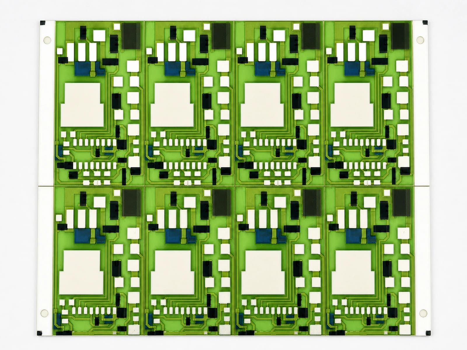
Overview
Surface finish is not a universal roughness number that can be copied from one alumina drawing to another. The functional interface starts with the named ceramic grade and forming route, continues through as-fired, lapped, ground, polished, or otherwise conditioned surfaces, and includes storage, handling, cleaning, paste wetting, leveling, drying, firing, refires, conductor overlap, protection, and later assembly loads. A surface may print sharply yet provide an unsuitable fired interface, while a rougher surface may increase mechanical keying but disturb line edges, thickness uniformity, local electric field, or fine-feature inspection. This guide organizes the decision around a controlled surface state and a production-intent material stack. It deliberately separates supplier typical roughness from measured incoming condition, visual cleanliness from chemical cleanliness, and initial adhesion from durability after thermal, mechanical, or environmental exposure. No finish, adhesion value, or preparation method is presented as a ThickFilmPCB capability until a drawing, named materials, process record, test method, and reviewed evidence packet agree.
Engineering review matrix
Each row links a design variable to evidence that can support a drawing or release decision.
| Variable | Control question | Verification route |
|---|---|---|
| Ceramic identity and forming route | Specify the exact alumina grade, supplier designation, lot, forming and firing condition, thickness, and functional face. | Check certificate and lot traceability, dimensions, appearance, and any agreed incoming material test without converting supplier typical data into a company claim. |
| Surface texture and waviness | Define roughness parameters, scan direction, filter, cutoff, waviness treatment, sampling locations, and treatment of pores or isolated defects. | Use a calibrated method and retain representative traces or maps with uncertainty and instrument settings. |
| Flatness, bow, and local support | Set datum, support condition, panel or part state, printing fixture, and allowable deformation during printing and assembly. | Measure in the specified support state and correlate print thickness or registration by position. |
| Cleanliness and time-to-print | Control particles, organics, ionic residue where relevant, cleaning media, rinse, drying, packaging, storage, and maximum exposed time. | Use agreed cleanliness witnesses and compare wetting, visual defects, and fired results by handling condition. |
| Paste and termination system | Name conductor, resistor, dielectric, protection, thinner, overlap, layer order, and supplier compatibility documents. | Review current technical data sheets and qualify the complete stack on the selected substrate condition. |
| Thermal process history | Record dry, burn-out, peak, time, atmosphere, furnace loading, cooling, refires, and later assembly heat without assuming one nominal setpoint describes the profile. | Use traceable profile records and compare fired thickness, appearance, resistance, and interface results. |
| Adhesion and durability method | Define coupon, bonded area, attachment material, fixture, load direction and rate, preconditioning, sample plan, failure categories, and acceptance rule. | Calibrate the force path, photograph or section failures, report individual values and censored results, and link records to the drawing. |
| Change-control boundary | List changes in ceramic, surface finishing, cleaning, paste, furnace, protection, joining, or environment that trigger review. | Maintain a revision-linked matrix and prevent unreviewed substitution even when nominal specifications appear similar. |
Controlled model
Surface-to-interface model with bounded measurements
Treat roughness, cleanliness, print transfer, and fired adhesion as linked but non-interchangeable observations. A single Ra value cannot describe peaks, valleys, waviness, porosity, chemistry, or the failure plane, so the model pairs surface metrology with printed coupons and a named post-fire test.
Ra = (1/L) ∫₀ᴸ |z(x)| dxArithmetic mean profile deviation over the evaluated length after the specified filtering and datum treatment.
- Units
- Ra and z in µm; evaluation length L in mm or µm
- Use boundary
- Ra is method-, cutoff-, direction-, and instrument-dependent. It does not by itself predict wetting, glass interaction, fired bond strength, or lifetime.
A_nom = W × L; σ_app = F_fail / A_nomA nominal apparent stress that can normalize a coupon failure load by the defined bonded footprint.
- Units
- A_nom in mm²; F_fail in N; σ_app in N/mm²
- Use boundary
- Use only when fixture geometry, loading mode, bonded area, cure or firing history, and failure classification are fixed. It is not an intrinsic adhesion property.
ΔR/R₀ = (R_after − R₀) / R₀Tracks electrical change of a witness feature after the selected conditioning or interface test.
- Units
- Dimensionless, commonly reported as % or ppm
- Use boundary
- Electrical stability is complementary evidence; it cannot identify the failure plane without microscopy or other agreed inspection.
Decision comparison
| Decision | Route A | Route B | Verification |
|---|---|---|---|
| As-fired versus mechanically finished surface | An as-fired surface preserves the ceramic supplier's native topography and may avoid finishing damage, but lot texture, bow, residue, and fine-feature transfer must be measured for the selected print. | Lapping, grinding, or polishing can change smoothness and flatness, while also changing exposed grains, subsurface damage, edge condition, particle burden, and cost. | Measure the same specified surface parameters and print identical production-intent coupons on separately traceable surface states before choosing either route. |
| Mechanical keying versus print definition | More texture may increase apparent mechanical interlock for some glass-containing systems, yet can increase thickness variation, conductor edge irregularity, and local void or coverage risk. | A smoother surface may improve fine-line imaging and inspection, yet cannot be assumed to provide adequate fired interaction or assembly durability. | Correlate profile data with wet-print transfer, fired microstructure, failure mode, and electrical response rather than optimizing either roughness or line appearance alone. |
- Record the failure plane: ceramic fracture, interface separation, cohesive paste failure, termination lift, solder or adhesive failure, and fixture failure mean different things.
- Supplier surface data remain grade-, size-, thickness-, and method-specific; incoming verification and change control still belong in the project plan.
Surface-interface qualification sequence
The order makes assumptions and ownership visible before a result is promoted to a requirement.
- 01
Define the functional interface
Identify which face receives each conductor, resistor, dielectric, or protection layer; state the required feature scale, electrical function, assembly method, environment, and failure consequences. Do not start with a preferred roughness value before the complete interface is understood.
- 02
Name the ceramic and surface route
Record alumina grade, supplier, forming and firing route, as-fired or finished state, finish direction, flatness, bow, edge treatment, packaging, shelf history, and any supplier change notice. Similar color or nominal purity does not make two substrates equivalent.
- 03
Specify surface metrology
Choose parameters, instrument, stylus or optical method, filtering, cutoff, evaluation length, scan direction, sampling map, datum, calibration, uncertainty, and treatment of pores or outliers. Retain raw traces where the decision depends on more than a summary value.
- 04
Control handling and cleaning
Map unpacking, gloves, fixtures, water and solvent quality, cleaning chemistry, rinse, dry, time-to-print, re-clean rules, particle control, and contamination witnesses. A visually clean surface can still carry residues that affect wetting or firing.
- 05
Print and fire representative coupons
Use named production-intent pastes, terminations, overlap, screen, dried thickness, furnace atmosphere and profile, refire count, protection, and witness geometry. Inspect wet and fired coverage so transfer defects are not mistaken for adhesion failures.
- 06
Test, classify, and release
Apply a defined loading and conditioning method, document failure plane and electrical response, include measurement uncertainty and sample rationale, and link acceptance to the drawing revision. Reopen qualification after a material, surface, cleaning, firing, or assembly change.
Failure controls
These are review prompts, not evidence that every risk applies or that every test is available.
- A
Selecting a finish from one supplier's typical Ra value without matching grade, measurement method, feature scale, or fired material system
- B
Treating visible cleanliness as chemical cleanliness and allowing handling residue or delayed printing to alter wetting
- C
Optimizing apparent adhesion while creating poor line definition, local thickness variation, trapped voids, or inspection ambiguity
- D
Reporting a pull value without bonded area, load direction, fixture, failure plane, conditioning, uncertainty, or individual results
- E
Mixing ceramic fracture, cohesive paste fracture, interface separation, attachment failure, and fixture failure into one average
- F
Releasing a surface condition from laboratory coupons that omit production refires, protection, assembly heat, mechanical load, or environment
Reference boundary
Public method sources
These sources support the engineering method and terminology used in this technical guide. They do not establish a ThickFilmPCB material list, capability limit, customer result, certification, or finished-product specification.
- 01KYOCERA — Standard Substrate Specifications
Supports that alumina substrate surface roughness, thickness, and camber are specified properties tied to named substrate products and conditions; the published values do not establish ThickFilmPCB incoming limits or adhesion.
- 02KYOCERA — Alumina packages and substrates
Supports grade- and process-dependent alumina substrate selection and the distinction between general substrate material and finished metallized construction; it supplies no thick-film adhesion guarantee.
- 03DuPont 5771 Gold Conductor technical data sheet
Supports treating substrate composition, screen printing, drying, firing, fired thickness, and bond conditions as one named-material test system; its laboratory values are not transferable to another paste or company process.
Inputs for a practical review
Unknown values may be labelled unknown. The review should convert uncertainty into an explicit decision or validation task.
Send Drawings- 01
Substrate drawing, alumina grade and supplier designation, thickness, flatness, functional face, edge state, and current surface-finish requirement
- 02
Conductor, resistor, dielectric, overglaze or overcoat, termination overlap, layer order, firing sequence, and allowed substitutions
- 03
Minimum printed features, registration, fired thickness, electrical function, inspection zones, and unacceptable surface or print defects
- 04
Cleaning, packaging, storage, time-to-print, handling, contamination, re-clean, and traceability expectations
- 05
Assembly stack, solder, braze, adhesive or wire-bond process, clamp and peel loads, rework, and later thermal exposures
- 06
Operating media, humidity, thermal cycling, vibration, shock, cleaning, corrosion, and required validation sequence
- 07
Surface measurement method, adhesion fixture, conditioning, sampling, acceptance rule, report fields, and change-control triggers